

● Grid modeling
● Curvature compensation
● Heat release
● Video overlay
● RST measurement
● In Situ microscope
Note: The selected image calculates tool convolution to minimize radius error. In this case, a 3mm tool was chosen.

Grid modeling

Curvature compensation

Heat release

Video overlay


In Situ microscope

New operating system dropdown
Advanced settings for digital zoom
Image capture timer and endpoint
Video capture curve and grid model
Loading and saving image enhancement formula
Standard configuration includes two 4K (UHD) cameras. Add a third 4K (UHD) microscope camera at the RST measurement location. It can be used with the newly added UT-F3 spectrometer.

The real-time view can be overlaid with saved X-ray or C-Sam images to further improve target localization.

Can be used for distributing and collecting polishing fluid, abrasives, and lubricants. The effective control of lubricating oil and particles greatly improves the quality of visual monitoring in the machining process.

| Product | Spectrometer type | Minimum film thickness |
| UT-F3 | 1280-1340nm NIR | 8 microns |
| UT-VIS | Visible light extension | 8 nanometers |
There are two options available for measuring the remaining silicon thickness (RST) in In Situ.


The new 4. X operating system provides users with interactive drawing to compare actual RST images with 3D models. This figure considers the three-dimensional mesh generated by surface contour, programmed X&Y curvature, and convolution generated by polishing drill bits due to their size and type.
After subsequent polishing iterations accompanied by modifications to the mesh model, the actual sample thickness and uniformity were approximated to the optimized model after final polishing.

Chip size X=15 mm Y=10 mm
5260.3 3mm diameter fine diamond tool
Spiral polishing pattern
Heat release at 80 ° C
Curvature compensation
Tool force=300g

Chip target camera view @ 50 microns+/-5

RST point contour map

RST diagram

Note: The selected image calculates tool convolution to minimize radius error. In this case, a 3mm tool was chosen.

Process conditions
5260.3mm diameter fine diamond cutting tool
5265.3mm diameter ultra-fine diamond cutting tool
Combination spiral and ASAP-1 polishing pattern
Curvature compensation
Polishing force=300g

Note: Additional polishing may be required. Measure RST and refine the 3D mesh after each cycle.
Process conditions5295.3 3mm直径Xylem刀具
2382.5 Blue Diamond Gypsum
2385.5 Yellow Diamond Gypsum
ASAP-1 series polished patterns
Polishing force=300g
Use 5299.3 Xybove 3mm cutting tool and silicon oxide/oxide
Aluminum undergoes final polishing

Total processing time=2 to 4 hours

The thermal modification of InSitu during sample preparation has long been proven to be a safe and effective method and tool for optimizing the uniformity of extreme silicon chips. Heat release can be used alone or in combination with curvature compensation and 3D mesh methods more frequently.

Hot table (6686.1) is a standard upgrade of ASAP-1 InSitu. It also adopts a hot plate mode for fixing/removing samples with crystal wax.

The stripe pattern on the same device prepared by Moir é at an increase in temperature shows an increase in final thickness uniformity.

Except for a series of processes based on time and pressure. ASAP-1 InSitu provides a unique set of electronic endpoint functions derived from capacitance/resistance.

By grounding the parts to the optional endpoint sample stage, the capacitance accumulation between the charged diamond tool and the embedding characteristics of interest (chip circuit, solder wire) can be used as an automatic termination function for the chip opening process.
This method can achieve fast, accurate, and reproducible endpoint processes without the need to spend time using optical microscopes.

The stripe pattern on the same device prepared by Moir é at an increase in temperature shows an increase in final thickness uniformity.
| Feature | Specifications |
| Z-Vertical Accuracy | The minimum step size is 0.04 micrometers (40 nanometers) |
| Workbench accuracy (X&Y stroke) | The minimum step size is 0.2 micrometers (200 nanometers) |
| Workbench travel range | 100mm x 100mm (max.) |
| Polishing method | Patent ASAP-1 floating head with Z-lock, enhanced by electronic sensors and tool modes (ASAP-1 Classic, ASAP-1 X, ASAP-1 switching, snake, user-defined X-Y, spiral, frame, and relief modes) |
| Sample tilt control | Automatic 2-turn tilt control (+/-5 degrees) |
| Force control | 1000 grams (maximum), 1gram precision. Total accuracy+/-10 grams |
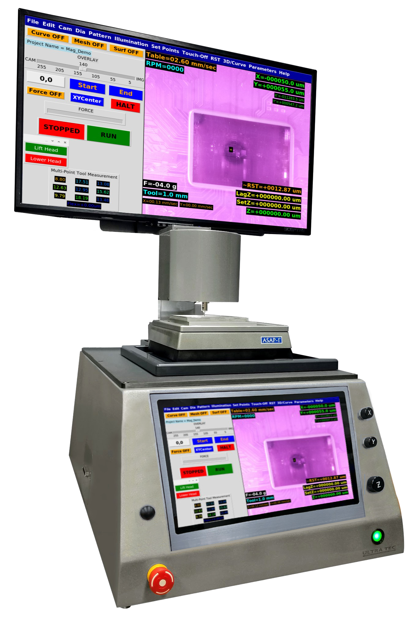
| Video | Real time 10.1-inch (255mm) touchscreen monitor, covering the sample stage and operating area. HDMI video output (optional) external monitor. 4.25-inch (108mm) auxiliary touch screen |
| Programming input method | Touch screen, joystick, and 3 physical rotary encoders. Optional wireless keyboard and mouse. File loading/saving to flash drive |
| Core software functions | The dropdown menu interface is used for file processing, camera selection, zoom and image enhancement, overlay, tool diameter, mode selection, force control, timer, lighting, set points, and triggering. Additional purchase options unlock RST, 3D control, heat, and endpoint detection in the menu. |
| Operate the camera | 4K UHD camera provides real-time video from 45 degrees to tool/surface interface |
| Target camera | 4K UHD camera provides top-down video for positioning and aiming |
| Power requirements | Universal: 100-120VAC; 200-240VAC (single-phase). Power consumption: up to 300 watts when in use |
| Size | 19 inches (480mm) wide x 27.5 inches (698mm) deep x 27 inches (685mm) high |
| Wight | 200lbs (91 kg) |
| Order Code | Project | Description |
6760.5 | ASAP-1® IN SITU (2019 ) | Digital selection area sampling system (100-240V, 50/60Hz). Including: X-Y worktable, tool spindle drive with sub micron Z resolution,+5/-5 degree automatic tilt worktable, integrated real-time machine vision, minimum 10 inch touchscreen LCD display, a set of 2mm and 3mm tools, and 6389.1 force feedback module. Two 4K ultra high definition cameras (target and process) |
6394.3 | 3D Module - Curvature and Mesh | System software upgrade, adding adaptive mesh coverage for processing and compensation of sample surface curvature. |
6686.1 | Heat release | Hardware and software upgrades to increase heat release capability. Touch screen control. PELTER based heating plate and chiller unit. Including cables and two mounting plates. Hot plate mode |
6675.1 | Machine Vision Monitor | 24 inch (minimum) monitor machine vision upgrade for improving on-site view of polishing head/sample surface interface, including mounting bracket (VESA) |
6677.1 | lubrication system | Automatic distribution and collection system for polishing fluid and abrasives |
| Feature module | ||
UT-F3 | RST measurement system | Non contact measurement of silicon and other semiconductors (1280-1340nm). Including: thickness calculation software. 4K camera (microscope); Si thickness standard. Note: The customer provides their own PC/tablet - requires Windows 10- with a measurement accuracy of approximately 10 microns |
UT-VIS | VIS extension module | The second "visible light" spectrometer can be added to the UT-F3 system to allow measurement up to approximately 10nm |
6368.1 | Capacitor/resistor terminal module | Hardware and software upgrades to increase endpoint pointing and improve opening performance |

 【 WeChat 】
Address:No. 501, Building 01, Northwest District, Suzhou Nano City,
No. 99, Jinjihu Avenue, Suzhou Industrial Park
Hotline:86-0512-62749825
Phone:86-18912625555 Mr Chen
Email:alan.chen@winwintek.com/ wuj@winwintek.com
Copyright © 2026 Win-Win Electronic Technology International Limited Su ICP NO.2025215884-1 Support:HuiCheng