

Empower intelligent manufacturing by making thermal failure nowhere to hide!
By combining refrigeration type detectors with lock-in amplification technology, the system can accurately capture weak thermal radiation signals, achieving high-sensitivity and high-resolution failure analysis, thermal diffusion measurement, and non-destructive testing.
Widely used in semiconductor and microelectronics manufacturing, chip level and package level failure analysis: locating chip short circuits, leakage, and functional failure areas; Electronic equipment and PCB detection, PCB board level failure localization: Quickly detect defects such as power short circuits, tin residues, solder pad cracks, etc., supporting wide field scanning; Display screens and consumer electronics: diagnose issues such as screen flicker, ESD static damage, and solder pad voids; Analysis of New Energy and Power Devices, Silicon Carbide (SiC) and GaN Devices: Leakage Path Localization, Thermal Distribution Optimization, Improving Device Reliability; Research on thermoelectric materials and batteries: evaluation of thermoelectric conversion efficiency, warning of battery thermal runaway, optimization of thermal management design; Fields such as scientific research and cutting-edge technology development.

Integrated core detection and analysis functions, lock-in function, maximum lock-in frequency of 25Hz, signal-to-noise ratio increased by more than 10 times
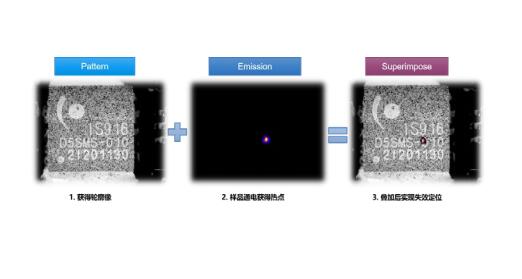
Designed functions that conform to engineering application habits, making operation easier and more convenient (overlaid with X-RAY diagram, OM diagram, BD diagram, PCB layout diagram; Video editing; 3D hotspot display and other functions.
Can be connected to an external power supply and testing machine
Can achieve full supply chain localization, break import dependence, and lead the industry in cost-effectiveness
Comprehensive and innovative high-quality after-sales service, innovative construction of deep calculation models for heat sources, cracking packaging black boxes
Example of overlay function

| Software features | IV testing function, hotspot/design pattern overlay function, video editing function, failure mode matching function, 3D view function, etc; |
| Phase locking analysis | Frequency ≤ 25Hz, thermal sensitivity less than 0.1mK |
Infrared camera | Medium wave 3-5 μ m, 640 * 512, 15um, MCT/InSb detector, cooling temperature less than or equal to 85K |
Objective lens | WA lens: adjustable field of view range from 38.4 * 30.72mm to 144 * 115.2mm (customizable for larger field of view) 1X lens: resolution: 15 μ m, NA: 0.125; 3X lens: resolution: 5 μ m, NA: 0.375; 8X lens: resolution: 2 μ m, NA: 0.8; 10X lens: resolution: 1.875um, NA: 0.8; |
Anti vibration system | VC-C level anti vibration system |
Motion Control | Vertical structure: electric mobile XYZ 200mm-200mm-300mm, repeat positioning accuracy ± 1um Longmen structure: electrically movable XYZ 50mm-50mm-100mm, with a repeatability accuracy of ± 1um Support multi-level objective lens switching, electrically switch 4 medium wave infrared lenses+1 optical lens (mechanical button+software control) |
Power supply | Supports external power supply and external triggering (dynamic analysis). Support simultaneous configuration of high voltage source and low voltage source Low voltage source 200V, 1.5A; High voltage source 3000V, 120mA |
Probe station | Standard 8-inch probe station as standard, optional high pressure/high temperature (room temperature to 200/300) probe station or double-sided probe station (4, 6, 8, 12 inch optional), including optical microscope and high-definition imaging camera for needle insertion |
Working conditions | Voltage: AC220V, vacuum greater than 50K Pa, compressed air: 0.6~0.8MPa |
Device dimensions | 1320mm * 1150mm * 1950mm, 1100kg (gantry structure) 1150mm * 1150mm * 1850mm, 650kg (vertical structure) |

 【 WeChat 】
Address:No. 501, Building 01, Northwest District, Suzhou Nano City,
No. 99, Jinjihu Avenue, Suzhou Industrial Park
Hotline:86-0512-62749825
Phone:86-18912625555 Mr Chen
Email:alan.chen@winwintek.com/ wuj@winwintek.com
Copyright © 2026 Win-Win Electronic Technology International Limited Su ICP NO.2025215884-1 Support:HuiCheng