

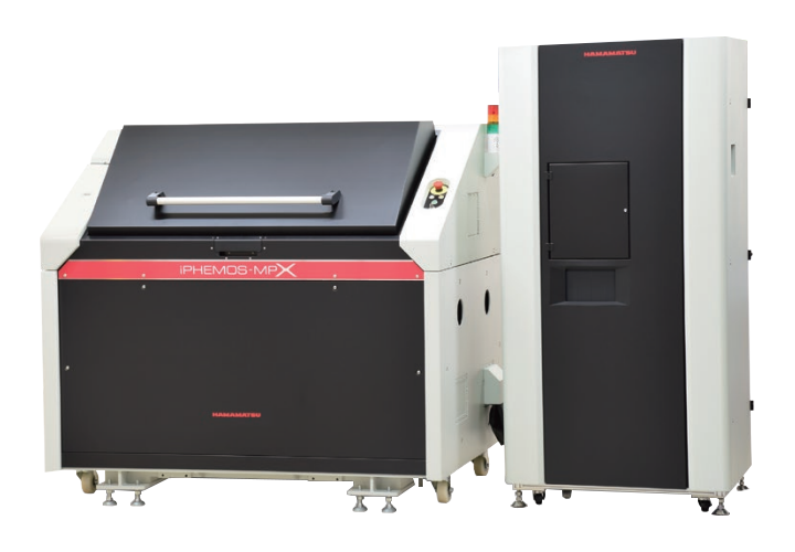
iPHEMOS-MPX is a high-resolution micro light microscope that can locate failure locations by detecting weak light and heat emitted by defects in semiconductor devices.
● Can install two ultra-high sensitivity cameras
● Up to 4 OBIRCH, DALS, EOP, and laser marking light sources can be installed
● Up to 4 OBIRCH, DALS, EOP, and laser marking light sources can be installed
● High precision stage designed specifically for advanced devices
By covering different emission analysis and thermal analysis detection wavelength ranges, it is easy to choose analysis techniques that match the sample and fault mode.
High sensitivity macro lens and up to 10 lenses, suitable for each detector sensitivity wavelength
| X | 60 mm |
| Y | 60 mm |
| Z | 60 mm |
*Due to the use of probe stations and interference from sample stations or NanoLens installations, the working range may be narrower than these values.

iPHEMOS-MPX overlays low light images onto high-resolution pattern images to quickly locate defect points. The contrast enhancement function makes the image clearer and more delicate.
The contrast enhancement function makes the image clearer and more delicate.
Display function
Comment: Comments, arrows, and other indicators can be displayed anywhere on the image as needed.
Scale display: The scale width can be displayed in segments on the image.
Grid display: Vertical and horizontal grid lines can be displayed on the image.
Thumbnail display: Images can be stored as thumbnails and called, and image information such as stage coordinates can be displayed.
Split screen display: It can display pattern images, low light images, overlay images, and reference images all at once on a 6-window screen.

TD Imaging
TD Imaging (optional) is a new technology suitable for identifying defects in complex structured semiconductors such as logic semiconductors. It can accurately locate defects through internal metal semiconductors.
| Size | Host: 1654 mm (W) × 1541 mm (H) × 1200 mm (D) * 1, approximately 1100 kg * 2 System/Instrument Rack: 880 mm (W) × 1841.5 mm (H) × 715 mm (D) * 1, approximately 300 kg Console * 3: 1000 mm (width) x 700 mm (height) x 800 mm (depth), approximately 39.2 kg (C16216-01 console)/1480 mm (width) x 700 mm (height) x 800 mm (depth), approximately 48.6 kg (C16216-02 console) |
| Line voltage | Single phase 200 V to 240 V |
| Power consumption | Approximately 3300 VA |
| Degree of vacuum | At least 80 kPa |
| Compressed air * 4 | 0.5 MPa ~ 0.7 MPa |
*1: Excluding protruding parts
*2: Including a sample stage
*3: Options
*4: Including regulators

 【 WeChat 】
Address:No. 501, Building 01, Northwest District, Suzhou Nano City,
No. 99, Jinjihu Avenue, Suzhou Industrial Park
Hotline:86-0512-62749825
Phone:86-18912625555 Mr Chen
Email:alan.chen@winwintek.com/ wuj@winwintek.com
Copyright © 2026 Win-Win Electronic Technology International Limited Su ICP NO.2025215884-1 Support:HuiCheng