

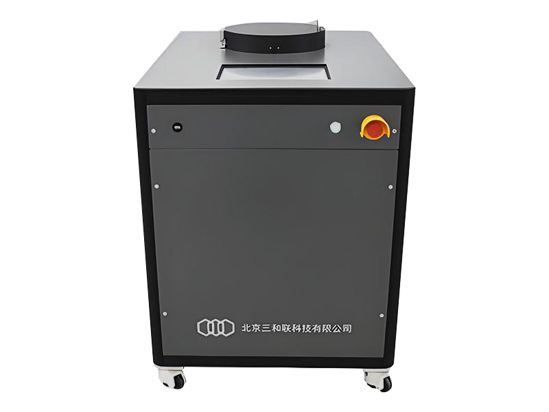
The reactive ion etching machine (RIE) series products independently developed by Beijing Sanhe Lian Technology Co., Ltd. are based on flat plate capacitive coupled plasma technology. The domestically produced RIE machines are suitable for patterned etching of silicon-based materials such as monocrystalline silicon, polycrystalline silicon, silicon nitride (SiNx), silicon oxide (SiO2), quartz (Quartz), and silicon carbide (SiC), and are high-quality products of domestic RIE machines.
Reactive ion etching (RIE) can be used to prepare micro nano structures and is a type of semiconductor manufacturing process technology. During the RIE etching process, various active particles in the plasma form volatile products with the material surface. These products are carried away from the surface of the material, ultimately achieving anisotropic microstructure etching on the material surface.
1. Support sample sizes: 4, 8, 12 inches, compatible with various small-sized samples, and support customization
2. RF plasma power range: 300/500/1000 W optional;
3. Molecular pump: 620/1300 l/s optional, optional with anti-corrosion pump set;
4. Front stage pump: mechanical oil pump/dry pump optional;
5. Pressure control: 0~1 Torr optional; Non pressure control mode configuration can also be selected;
6. Process gas: Up to 9 process gases can be equipped simultaneously;
7. Gas range: determined according to user application requirements and system design, selectable within the range of 0~1000 sccm;
8. Sample temperature control: 10 ° C~room temperature/-30 ° C~room temperature/customizable temperature range;
9. Back helium cooling can be configured according to the application;
10. Detachable anti pollution lining;
11. Load lock is optional;
12. Fully automatic one key control system;
1. Silicon based materials: silicon (Si), silicon dioxide (SiO2), silicon nitride (SiNx), silicon carbide (SiC)
2. III-V materials: Indium Phosphide (InP), Gallium Arsenide (GaAs), Gallium Nitride (GaN)
3. II-VI material: cadmium telluride (CdTe)
4. Magnetic/alloy materials
5. Metal materials: aluminum (Al), gold (Au), tungsten (W), titanium (Ti), tantalum (Ta)
6. Organic materials: photoresist (PR), organic polymers (PMMA/HDMS), organic thin films
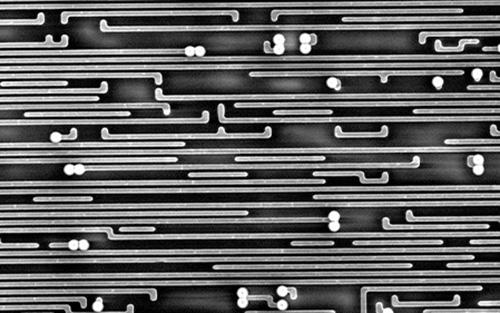
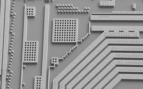
1. Silicon based materials, nanoimprint patterns, array patterns, and lens pattern etching;
2. Room temperature etching of indium phosphide (InP), patterned etching of InP based devices in optical communication, including waveguide structures, resonant cavity structures, and ridge structures;
3. SiC material etching, suitable for microwave devices, power devices, etc;
4. Physical sputtering etching is applied to certain metals, such as nickel (Ni), chromium (Cr), ceramics, and other materials that are difficult to etch chemically. It achieves patterned etching of the materials through physical bombardment;
5. Organic material etching is applied to the etching, cleaning, and removal of organic materials such as photo resist, PMMA, HDMS, and polymer;
6. Failure Analysis FA: Layer removal and etching of chips;
7. Two dimensional material etching: W, Mo two-dimensional material, graphene;
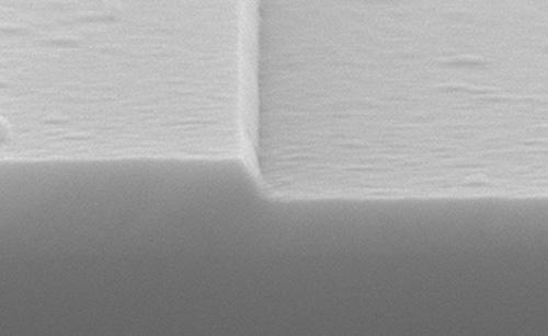
Quartz material step etching, step height: 300 nm, etching rate: 90 nm/min
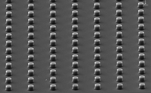
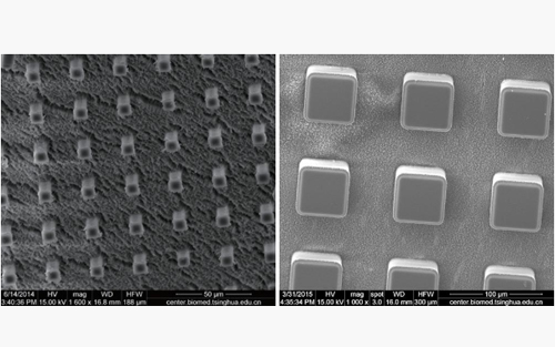
Silicon material micro array etching for surface hydrophilic and hydrophobic modification
InP room temperature etching, laser application, ridge structure etching, etching rate: 200 nm/min
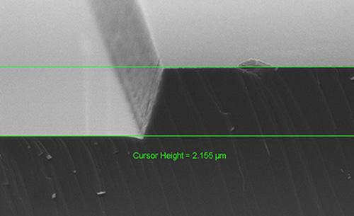
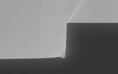
Silicon carbide step etching, etching depth: 2 μ m, etching rate: 220 nm/min
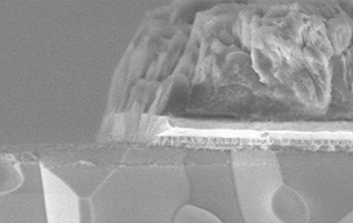
Etching of metal ceramic thin film material (Au/Ni/Cr/Al2O3), etching depth: 500 nm, etching rate: 15 nm/min
SiO2 delamination etching, perforated results, chip failure analysis, etching rate: 100 nm/min
SiO2 delamination etching without holes, chip failure analysis, etching rate: 100 nm/min
SiO2 is used for etching and removing organic compounds such as photoresist (PR), PMMA, HDMS, polymer, etc

 【 WeChat 】
Address:No. 501, Building 01, Northwest District, Suzhou Nano City,
No. 99, Jinjihu Avenue, Suzhou Industrial Park
Hotline:86-0512-62749825
Phone:86-18912625555 Mr Chen
Email:alan.chen@winwintek.com/ wuj@winwintek.com
Copyright © 2026 Win-Win Electronic Technology International Limited Su ICP NO.2025215884-1 Support:HuiCheng