

The perfect combination of unique leak free magnetic ultra-high resolution SEM and plasma FIB, with high precision and efficiency, provides the most comprehensive solution for multimodal material characterization and TEM sample preparation
● Using TESCAN's unique multimodal 3D FIB-SEM tomography technology, energy dispersive spectroscopy (EDS), backscattered diffraction (EBSD), and time-of-flight secondary ion mass spectrometry (ToF SIMS) data can be synchronously obtained during the FIB continuous cutting process to characterize and analyze the sample structure, element distribution, chemical composition, and isotopes in three dimensions.
● The BrightBeamTM leak free ultra-high resolution electron tube provides ultra-high resolution imaging and nanoscale analysis for various materials, with a low landing energy feature specifically designed for sensitive materials to protect samples from damage.
● Equipped with high-performance Mistral ™ The xenon plasma FIB tube provides an ion beam current of up to 3.3 μ A and a resolution better than 10nm, ensuring fast and accurate three-dimensional characterization of any sample. In addition, high-quality surface treatment can be achieved in areas of user interest.
● Mistral ™ The excellent resolution and beam density of the plasma FIB tube, combined with the fully automated TEM sample preparation module - TEM AutoPrep ™, Users can prepare TEM samples as conveniently as using gallium ion FIB, without worrying about interference from gallium ion implantation.
● Adopting TESCAN's unique swing sample stage technology, combined with Mistral ™ The high beam characteristics of plasma FIB tube enable the rapid acquisition of high-quality data even for challenging samples such as SiC, ceramics, graphite anodes, etc., while ensuring the surface quality of the samples.
● TESCAN swing sample stage technology can solve the artifact problem caused by the "curtain phenomenon", significantly improving the efficiency of large volume 3D characterization and cross-sectional cutting, while ensuring excellent surface quality; The TESCAN TRUE-X-sectioning technology is capable of preparing cross-sections 1 millimeter wide on large volume samples, providing strong support for in-depth material analysis.
● Achieve unmanned and multi-point batch TEM sample preparation, allowing operators more time to handle other tasks while significantly improving throughput and work efficiency. This feature supports preparation at different locations and on multiple samples, and can adapt to running at any time, even overnight.
● Utilize AutoSlicer ™ The intuitive template, which includes various editable attributes such as material type and etching rate, enables the preparation of high-quality TEM samples from multiple materials, meeting the high standard requirements of (S) TEM analysis.
● Use an integrated argon ion wide ion beam for final polishing to ensure that the sample remains intact in vacuum while preparing high-quality and minimally damaged TEM samples.
● Integrated TESCAN OptiLift ™ Nano manipulator, combined with intuitive control software, can prepare high-quality TEM samples through flat cutting, reverse cutting, or other methods without opening the sample chamber. Accurate positioning ensures the best results in (S) TEM microscopic analysis of the samples. The simplified operation process greatly improves work efficiency and makes operations easier and more convenient.
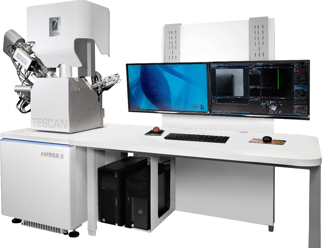
TESCAN AMBER X2 has achieved a revolutionary leap in the field of FIB-SEM technology, perfectly integrating the high precision of gallium ion FIB-SEM and the high efficiency of plasma FIB-SEM. The innovative solution provides superior high resolution, making the accuracy of plasma FIB-SEM comparable to that of gallium ion FIB-SEM. In addition, TESCAN AMBER X 2 is capable of quickly completing large volume milling and obtaining high-quality multimodal 2D and 3D data in areas of hundreds of micrometers.
The TESCAN AMBER X 2 is equipped with the latest generation MistralTM plasma FIB tube, which can more accurately and efficiently process various materials. A higher beam density ensures excellent resolution and outstanding performance even at low acceleration voltages. FIB ion beam current can reach up to 3.3 µ A, achieving efficient material processing. The leakage free BrightBeamTM ultra-high resolution electron tube provides high-quality imaging effects and is suitable for characterizing various materials, including magnetic or non-conductive materials.
In addition, TESCAN AMBER X 2 integrates fully automated TEM sample preparation software, simplifying the operation process and improving the efficiency of sample preparation. Both beginners and expert users can easily control it. The workflow is fully automated, eliminating the need for real-time monitoring by users and enabling efficient preparation of TEM samples.
TESCAN AMBER X 2 can be optionally equipped with 3D ToF SIMS (time-of-flight secondary ion mass spectrometer), 3D EDS (energy dispersive spectroscopy), 3D EBSD (backscatter diffractometer), and various imaging software, forming a comprehensive solution that is most suitable for comprehensive material characterization. This solution can cover multidimensional analysis from nanometer to micrometer scales, providing users with profound insights into their material structure and composition.
TESCAN AMBER X 2 continuously explores the best performance that FIB-SEM can achieve, combining precision and efficiency, enhancing research and analysis capabilities in the field of materials science, and laying the foundation for innovative discoveries.

▪ Schottky field emission filament, ensuring a service life of up to 2 years
▪ Electromagnetic electrostatic composite objective lens
▪ Electron accelerator inside the tube
▪ Multi mode SE and BSE detectors inside the lens barrel
▪ Electron beam landing energy: 50 eV – 30 keV (<50 eV * under electron beam deceleration technology)
▪ Optimizing beam spot by controlling electromagnetic aperture
▪ Probe current: 2 pA-400 nA, continuously adjustable
▪ Field of view: 7 mm @ WD=6 mm,>50 mm @ maximum WD
▪ Maximum magnification: 2-2000000 times
▪ Xenon plasma source (ECR), the lifespan of the ion source is affected by actual usage conditions
▪ Configure piezoelectric driven aperture converter, 30 aperture aperture
▪ Electrostatic beam gate, equipped with Faraday cup
▪ Ion beam energy: 500 eV -30 keV
▪ Probe current: 1 pA-3.3 µ A
▪ Maximum field of view: 1 mm
▪ SEM working distance at the overlap point: 6 mm
▪ FIB-SEM angle: 55 °
▪ 1.4 nm @ 1 keV (无漏磁)
▪ 1.3 nm @ 1 keV (减速模式)*
▪ 0.9 nm @15 keV (无漏磁)
▪ 0.8 nm @ 30 keV STEM* (无漏磁)
▪ 1.8 nm @ 30 keV, GSD detector*
▪ 3.0 nm @ 3 keV, GSD detector*
▪ 10 nm@ 30 keV
▪ X&Y axis travel: 130 mm
▪ Z-axis travel: 96 mm
▪ Tilt: computer-controlled center type, -70 ° to+90 °
▪ Rotation: computer-controlled center type, 360 ° (continuously adjustable)
▪ Maximum sample height: 92 mm (can reach 133 mm without rotation)
▪ Maximum sample size: diameter 180 mm, XY axis movement and rotation are not affected, cannot tilt (placing larger samples may limit movement and rotation)
▪ Maximum sample weight: 8000g
▪ 1000 g (XYZRT fully movable)
▪ 8000 g (XYZ is fully movable)
▪ Installation of Rocking Stage: 500g
▪ Cradle style sample stage
Note: The actual travel of the movement depends on the actual configuration and the working distance or Z-axis value at that time.
▪ Width: 340 mm
▪ Depth: 315mm
▪ Number of interfaces: 20+
▪ Vibration isolation method: active (built-in)
▪ Expansion: Used for 6 "and 8" wafers*
▪ Expansion: Used for 6 ", 8", and 12 "wafers (requires installation of a cradle style sample stage)*
▪ Extension: Combined Raman Spectrometer (RISE) ™)*
▪ Infrared camera for observing the internal conditions of the sample room
▪ The second infrared camera*
▪ Integrated plasma cleaner
▪ High vacuum:<9 x 10⁻³ Pa
▪ Low vacuum (N2) */MultiVac (N2, H2O) *: 7-500 Pa
▪ Pre stage vacuum pump: oil-free dry pump
▪ Sample pre extraction room*
▪ Pian meter, including anti-collision alarm function
▪ Everhart Thornley detector (E-T) in the sample room
▪ Multi mode detector (MD) inside the lens barrel
▪ Axial BSE/SE detector inside the tube
▪ Low vacuum secondary electron detector (GSD), used under variable vacuum MultiVac*
▪ Secondary Ion Detector (SITD)*
▪ Scalable high sensitivity scintillation type backscattered electron detector (LE-BSE)+
▪ Scalable scintillation backscattered electron detector (R-BSE)*
▪ Scalable high sensitivity four segment solid-state backscattered electron detector (4Q LE-BSE)*
▪ Scalable scintillation water-cooled backscattered electron detector, heat-resistant temperature<800 ° C, (Water Cooled BSE)*
▪ Scalable scintillation aluminum plated backscattered electron detector, capable of simultaneously receiving cathode fluorescence and backscattered electron signals, (Al-coated BSE *)
▪ Scalable integrated cathode fluorescent detector (CL), 350-650 nm*
▪ Scalable integrated cathode fluorescent detector (CL), 185-850 nm*
▪ Scalable integrated 4-channel color cathode fluorescent detector (Rainbow CL *)
▪ Scalable Scanning Transmission Electron Detector (HADF R-STEM *), capable of receiving bright field (BF), dark field (DF), and high angle dark field (HADF) signals, with up to 8 TEM copper grids placed
▪ Optical navigation and integrated camera (ONCam) * 2
▪ EDS * (third-party) spectrometer requires shutter
▪ Backscatter electron diffractometer EBSD * (third-party)
▪ Spectrometer WDS * (third-party)
▪ Integrated Time of Flight Secondary Ion Mass Spectrometer TOF-SIMS*
▪ Confocal Raman Spectrometer (RISE) ™)*
OptiGIS ™*: Scalable single gas injection system
▪ Up to three OptiGIS can be configured ™ Injection system (multiple gas sources to choose from)
*Optional,+recommended option * 2 to achieve image navigation for samples no higher than 40mm
▪ Platinum Metal Deposition (Pt)+
▪ Tungsten metal deposition (W)*
▪ Carbon deposition (C)*
▪ Insulator deposition (SiOx)*
▪ Enhanced etching (H2O)*
▪ Enhanced Etching (XeF2)*
▪ Special gas for planar IC delamination*
▪ Other gases can be selected as needed*
▪ TESCAN OptiLiftTM (XYZR) *
▪ TESCAN Nanomechanical Arm (XYZ)+
▪ Swinging sample stage, can remove curtain effect+
▪ True-X cross-sectional mask, used for high-quality sample cross-sectional processing+
▪ Nanomechanical arm (third-party)*
▪ Charge neutralization gun (used for FIB charge compensation)*
▪ Pneumatic Shutter with Energy Spectrum*
▪ Electrostatic beam gate of SEM tube*
▪ TESCAN EssenceTM EBL Kit*
▪ TESCAN FlowTM EBL offline version*
▪ Residence time: 20 ns -10 ms, step or continuous adjustable
▪ Full image scan, selected area scan, line or point scan
▪ Image rotation, movement, and tilt compensation
▪ Frame accumulation, line accumulation
▪ DrawBeam ™, Digital graphic generator, 16 bit DAC
▪ Dynamic Focus
▪ Frame Accumulation Drift Correction (DCFA)
▪ Maximum image pixels: 16k x 16k
▪ Image aspect ratios: 1:1, 4:3, and 2:1
▪ Image stitching, panoramic image size has no maximum limit (requires automatic stitching software)*
▪ Capable of supporting up to 8 real-time signal channels simultaneously
▪ Real time pseudo color image and multi-channel signal mixing
▪ Image formats: TIFF, PNG, BMP, JPEG, and GIF
▪ Dynamic range: 8 or 16 bits
▪ Keyboard and Mouse
▪ trackball
▪ Multi functional control panel+
▪ TESCAN Electron Microscope Special Control Software Essence ™
▪ High performance configuration: Intel Core i7 or equivalent processor, 32GB memory, 4 TB HDD hard drive, Nvidia GTX1660 or equivalent graphics card, Windows 11 Pro 64 bit (detailed information can be provided upon request)
▪ 32 "QHD monitor
▪ Highly customizable interface layout
▪ Customizable Function Keys (F-keys)
▪ Multi user account management
▪ Quick search bar
▪ Revoke and redo function
▪ Real time display of single, double, four or six images
▪ Multi channel real-time pseudo color image
▪ SEM electron gun and FIB ion gun automatically start
▪ Alignment of electron gun and electron tube
▪ Contrast brightness
▪ Automatic aggregation, automatic astigmatism correction, automatic objective lens centering
▪ In-FlightBeamTracing ™ Realize optimization of electron beam and ion beam
▪ Optimization of Electron Beam Spot
▪ Optimization of ion beam spot
▪ Set FIB-SEM image overlap point
▪ GIS nozzle position and temperature control
▪ Automatic FIB setting optimization
▪ Measurement software, tolerance measurement software
▪ image processing
▪ preset parameters
▪ Histogram and LUT
▪ SharkSEMTM Standard Edition (Remote Control)
▪ 3D anti-collision modeling software
▪ Object area
▪ Optoelectronic combination
▪ DrawBeamTM Electron Beam Writing Software Expert Edition
▪ Scheduled shutdown
▪ FIB-SEM 3D reconstruction*
▪ FIB-SEM 3D Reconstruction Professional Edition */Multimodal Edition*
▪ automatic slicing ™*
▪ TEM AutoPrep*
▪ TEM AutoPrep Pro*
▪ CORAL ™ (Electron microscopy software module for life sciences)*
▪ Automated electron beam writing software (DrawBeam) ™ Automate)*
▪ Automatic puzzle software*
▪ Sample observation*
▪ Low angle polishing*
▪ Automatic segmentation * (please verify if unsure)
▪ FIB-SEM Expert PI (Python Script Editor)*
▪ System check*
▪ Synopsys client*
▪ TESCAN Flow ™ (Offline processing software)*
▪ TESCAN Delayering module
*Optional,+Recommended Optional Items
▪ Power supply: 230 V ± 10%/50 Hz (120 V/60 Hz - optional), power of 2300 VA, standard configuration of one 2 kW UPS.
▪ Compressed air: 5-7 bar (73-102psi), required to be clean, dry, and oil-free.
▪ Compressed nitrogen gas for vacuum release: 1-7 bar (15-102 psi), with a purity of 99.99% or better (4.0 N).
▪ Compressed xenon gas: 300 kPa (3 bars).
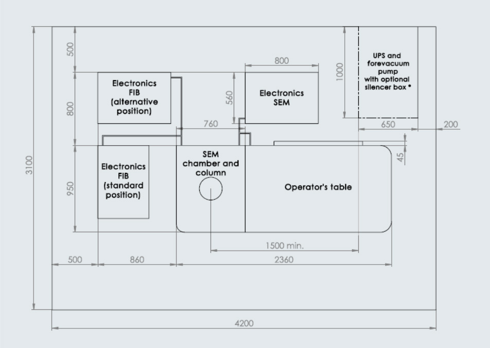
▪ Installation space: minimum space of 4.2 × 3.1 m; door width not less than 1.0 m.
▪ Environmental temperature: 17-24 ° C, with stable temperature changes within 2 ° C and hourly temperature fluctuations of less than 1 ° C
▪ Relative humidity:<65%
▪ Environmental magnetic field: synchronous<300 nT, asynchronous<100 nT
▪ Vibration:<10 μ m/s (below 30 Hz),<20 μ m/s (above 30 Hz)
▪ Noise: less than 60 dBC
▪ Altitude: not higher than 3000 meters
1. Site measurements must be conducted by technicians authorized by TESCAN. The parameters of the magnetic field will be affected by the actual acceleration voltage, and the acceleration voltage measured here is 20 kV.
▪ Basic training: TESCAN engineers complete on-site installation of equipment.
▪ Advanced training (optional): TESCAN China demonstration center or user site.
*If the mechanical pump and TESCAN AMBER X 2 electron microscope are placed in the same room, it is recommended to purchase a TESCAN static speaker (ordered separately) along with the electron microscope.
© TESCAN GROUP, a. s.
TESCAN AMBER X 2 is an upgraded model based on TESCAN S8000 X.
TESCAN technology is protected by patents, such as WO2015003671A3, CZ301692B6, US2015279616A1,CZ28392U1, US9721781B2, US10886139B2,
US2019074184A1, WO2019185069A1, WO2021244685A1, CZ2020474A3, etc.
BrightBeam ™, Wide Field Optics ™, In-Flight Beam Tracing ™, DrawBeam ™, TESCAN Essence ™, Mis t ral ™, OptiGIS ™ And EquiPower ™ All are TESCAN
The trademark of GROUP, a. s.
RISE ™ It is a trademark of WITec Wissenschaftliche Instrumente und Technologie GmbH.
Windows ™ It is a trademark of Microsoft Corporation.

 【 WeChat 】
Address:No. 501, Building 01, Northwest District, Suzhou Nano City,
No. 99, Jinjihu Avenue, Suzhou Industrial Park
Hotline:86-0512-62749825
Phone:86-18912625555 Mr Chen
Email:alan.chen@winwintek.com/ wuj@winwintek.com
Copyright © 2026 Win-Win Electronic Technology International Limited Su ICP NO.2025215884-1 Support:HuiCheng