

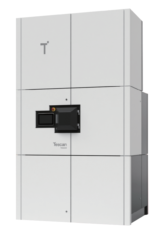
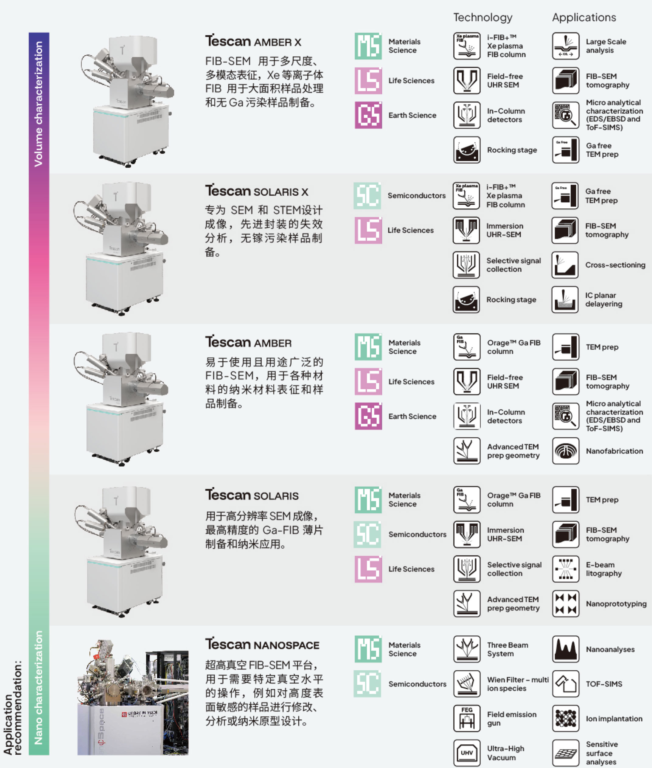
The first integrated, spiral assisted analytical near ultra-high vacuum 4D-STEM
TESCANTENSOR is the world's first professional 4D-STEM for multimodal characterization of the nano morphology, chemical, and structural properties of functional materials, films, natural and synthetic particles, with outstanding 4D-STEM performance and unprecedented universality.
4D-STEM is a microscopy technique that truly achieves multimodal characterization of the characteristics of nanoscale materials, such as morphology, chemistry, and structure. On each pixel in the STEM dataset, TESCAN TENSOR can quickly and perfectly synchronize diffraction patterns and energy spectra, revealing all the information about electron beam sample interactions, thus obtaining material properties more widely.

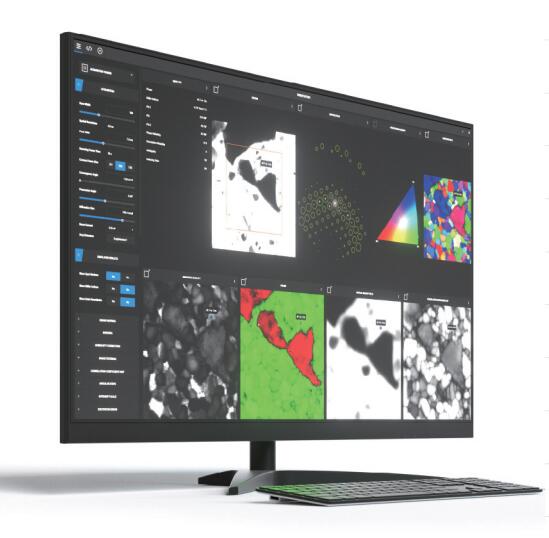
TESCANTENSOR's truly unique feature is Explore, which is TENSOR's integrated platform for (near) real-time processing and analysis of large-scale scanning diffraction pattern datasets. Explore can assist materials scientists, semiconductor researchers, failure analysis engineers, and crystallographers in achieving 4D-STEM measurement capabilities without requiring specialized knowledge in STEM optics or 4D-STEM data analysis and post-processing.

The TESCAN TENSOR 4D-STEM is capable of ultra fast and precise synchronization for direct electron diffraction imaging, energy dispersive spectroscopy (EDS) acquisition, electron beam, electron beam shutter, and real-time analysis and processing of collected data.
By integrating the most advanced technologies and components currently available, we can achieve:
● Hybrid pixel direct electron diffraction camera (DED)
● Sample area near ultra-high vacuum
● Progressive Electron Diffraction (PED)
● Fast and integrated electron beam shutter
● Large solid angle, symmetrical, windowless energy spectrum
● Near real-time 4D-STEM analysis and processing software (Explore)

Scientists, engineers, technicians, or students have always wanted an easy-to-use TEM solution that can be used without the need for weeks or months of complex electronic optical path adjustment and calibration training. TESCAN TENSOR allows you to spend your time on how to characterize samples, rather than on optical path tuning. This is achieved through the implementation of "measurements" with preset optical characteristics, such as beam current, convergence angle, spot size, and precession on or off - automatic adjustment and alignment.
Conclusion: This is an analytical 4D-STEM that is as user-friendly as TESCAN scanning electron microscopy, possessing all the advantages and benefits of a result oriented electron microscope. This will also bring economic benefits, such as newcomers or new users being able to use the device more quickly and efficiently, resulting in higher utilization rates and quick return on investment.

4D-STEM (4D Scanning Transmission Electron Microscopy) is the development direction of Scanning Transmission Electron Microscopy (STEM), which fully utilizes the innovation of mixed pixel direct electron detectors to capture the electron diffraction patterns of each pixel in STEM images. Using this method, when the electron beam scans the 2D region of interest (ROI) in real space, the detector can easily obtain the 2D reciprocal spatial information (electron diffraction pattern) of each pixel, hence it is called 4D-STEM.
But TESCAN TENSOR went further and obtained EDS spectra and electron diffraction patterns for each pixel in the 4D-STEM dataset. We refer to this unique capability as analytical 4D-STEM. The combination of analytical 4D-STEM and more traditional STEM and STEM tomography provides a comprehensive solution for characterizing functional materials, thin films, synthetic or natural nanocrystals.
Left image: EDS elemental diagram, with red representing carbon and green representing iron. The energy spectrum shows that the metal particles inside the carbon nanotube are iron.
Left image: STEM bright field image, showing the deformation of nickel alloy single crystal under indentation.
Left image: ADF image of lithium titanium phosphate anode particles.

Nanobeam diffraction (NBED) patterns can provide crystal information of carbon nanotubes and the metal particles they encapsulate.
The crystal orientation diagram of nickel alloy with recrystallization and changed orientation shows that the grain orientation has shifted from [001] to [03].
Phase diagram and orientation diagram of titanium oxide (TiO2) particles distributed along the grain boundaries of phosphate anodes
TESCANTENSOR offers a range of optimized, multi-mode, "out of the box" STEM, 4D-STEM, and tomography measurements. Applying these to samples is as simple as pressing a button, without requiring you to have extensive experience in (S) TEM optical adjustment and alignment, scanning electron diffraction data acquisition, or 4D-STEM data analysis and processing.
Mainly used for sample navigation and feature size measurement, the integrated scintillation based bright field and circular dark field/high angle circular dark field detector can quickly obtain STEM images up to 1 gigapixel (up to 10 gigapixels/second).
STEM lattice imaging measurements with automatic assisted alignment can be used to obtain atomic resolution bright field (as low as 2.8A) and high angle circular dark field (as high as 3.5A) STEM images.
Thanks to two symmetrically arranged windowless EDS detectors with a solid angle of 2Srad, element maps can be obtained at high EDS counting rates (>>10Ocps). Qualitative and quantitative EDS analysis are fully integrated into the user software.
Select orientation/phase measurement for near real-time orientation analysis and phase analysis of single-phase, multi-phase polycrystalline, and amorphous materials. A small electron beam (as low as 1nm) scans the sample, while obtaining diffraction patterns at a speed of thousands of frames per second and automatically indexing them in real-time. Electron beam rotation can be achieved by pressing a button, significantly improving the quality of the results.
Strain measurement combines nano beam electron diffraction with electron beam precession to achieve high-precision strain maps in single crystals. Once the grains are tilted to the positive band axis through automated sample tilting, a small (as low as 1nm) rotating electron beam will scan the crystal and obtain thousands of diffraction patterns. Spinning improves the quality of diffraction patterns used for strain analysis by presenting more diffraction spots and producing more uniform spots. The strain map is then gradually analyzed to provide operators with almost real-time strain information.
Virtual STEM is a highly configurable 4D-STEM measurement that allows for real-time reconstruction and visualization of STEM images from 4D-STEM datasets. Users can directly define virtual light spots or circular apertures on the obtained diffraction patterns and use these apertures to reconstruct images. Alternatively, analyzing the 4D-STEM dataset can be exported to open-source pixelated STEM data analysis and processing platforms such as HyperSpy, LiberTEM, or Py4DTEM.
STEM and STEM-EDS are two measurement methods used for acquiring and reconstructing 3D morphology (STEM) or element distribution (EDS) datasets for subsequent analysis and visualization in a range of 3D imaging software, including TESCAN's 3D volume analysis software.
TESCANTENSOR can also be used for 3DED (micro ED) diffraction imaging acquisition and analysis. Regardless of whether there is precession or not, almost parallel nanobeams can be focused onto a spot as small as 20 nm, and diffraction patterns can be obtained as the sample gradually tilts to a larger range of angles. This provides a superior solution for the structural analysis of synthetic or natural submicron and nanometer sized particles. The optional PETS Advanced software can be used to analyze the 3D spiral electron diffraction (3DPED) dataset to generate unit cell sizes.
The performance, usability, and even availability of 4D-STEM measurements have been affected throughout history because they were not originally designed for this purpose due to the lack of integration of 4D-STEM components in the (S) TEM tube. But TESCANTENSOR is not like that.
Synchronization of electron beam scanning:
● EDiffraction imaging
● EDS acquisition
● EElectron beam rotation
● Quick beam brake
● ENear real-time 4D-STEM data analysis and processing
Combined with powerful software solutions, TESCANTENSOR is a microscope specifically designed for analyzing 4D-STEM applications.

TENSOR's integrated component is the QUADRO direct electronic detector from DECTRIS, a leading developer and manufacturer of precise, high-performance hybrid pixel X-ray and electronic detectors. The properties of DECTRIS QUADRO, particularly its large detector size (512x512 pixels), sensitivity, and speed( 2250fps@16 The position makes the detector the most suitable for 4D-STEM applications with screw in assistance.
In the absence of dynamic diffraction artifacts (i.e. prohibited reflection), the generated spiral electron diffraction patterns are highly suitable for various applications. The benefits include better differentiation of diffraction patterns during orientation and phase analysis, or improved accuracy of strain maps. TESCANTENSOR | Use NanoMEGAS' validated and trusted ASTAR software algorithm for template creation and pattern indexing.
Higher order reflection also improves the structural determination of nanocrystalline materials. For structural determination using spiral assisted electron diffraction tomography (3DED with spiral or 3DPED), TESCANTENSOR offers the optional PETS Advanced software, which is a version of FZU's PETS software (PETS. FZU. cz) customized for TESCAN.
The integration of electron beam precession is a key feature of TESCANTENSOR. The ability of electron beam rotation means that the incident electron beam is tilted and continuously rotates around the central axis of the microscope. The rotation of the electron beam must be carefully aligned to ensure that the rotation axis coincides with the surface of the sample, and the electron beam converges on the smallest circular point possible. Due to the unique barrel design and software automation integrated into the basic design of TESCANTENSOR's new system architecture, this alignment can be effortlessly achieved automatically.
TESCANTENSOR allows you to easily manipulate electron beam precession and non precession throughout the entire 4D-STEM measurement range, especially for orientation and phase diagrams as well as strain maps, and also for virtual STEM and diffraction tomography. The precession causes the Ewald sphere to oscillate in the inverted space, which leads to many positive factors:
● Minimize dynamic effects while maintaining the geometric shape of the diffraction pattern;
● Compared to static Ewald spheres, there are more reflections in the zero order and high-order Laue regions (ZOLZ and HOLZ);
● The intensity is integrated through the Bragg condition and is not dominated by complex contrast patterns.


TESCANTENSOR is equipped with two symmetrical windowless EDS detectors with a solid angle of 2Srad to achieve high counting rate measurements, such as composition (elemental map), EDS tomography or virtual STEM, in order to obtain the original 4D-STEM dataset, which not only contains the diffraction patterns of each pixel in the dataset, but also EDS spectral information.
The design of the TESCANTENSOR tube includes modular ultra-high pressure components such as ConFlat (CF) flanges and copper gaskets to achieve a vacuum degree of 10 Pa in the sample area. This actually eliminates the contamination of the sample by hydrocarbons present in the vacuum of the tube.
When designing TESCANTENSOR, we found that compared to systems with multiple components on traditional TEM platforms, better integration is needed between microscopes, detectors, samples, users, and even science. We propose the concept of a "sample/result centered" system, rather than the more traditional "instrument centered" system. If the focus should be on the samples and results, rather than on the instrument, then the operation of the instrument must be transparent to the user. The result is that scanning transmission electron microscopy is designed for measurement, rather than having to design a measurement solution for the microscope.
No set of applications can benefit more from application driven design than the resurgence of 4D-STEM and electron diffraction. The unique feature of 4D-STEM is that once you have a scanning diffraction dataset, you can extract information from it through software analysis and processing. You can draw strain and electric field intensity maps very accurately. You can obtain crystal orientation diagrams and phase diagrams. It is precisely this that makes us very transparent to users who are not experts in electron microscopes. Choose any of these measurements, and the tool will automatically process them while processing the extracted information in near real-time. This allows you to spend time on valuable samples without being hindered by complex setup processes and achieve optimization results in the shortest possible time. For traditional researchers engaged in basic sciences, application driven design is not a problem, but in the growing materials science market, both academia and industry see a desire for "tools" rather than "instruments". This is particularly important for ensuring utilization and productivity to support you in obtaining investment returns from increasingly complex scientific instrument purchases.

 【 WeChat 】
Address:No. 501, Building 01, Northwest District, Suzhou Nano City,
No. 99, Jinjihu Avenue, Suzhou Industrial Park
Hotline:86-0512-62749825
Phone:86-18912625555 Mr Chen
Email:alan.chen@winwintek.com/ wuj@winwintek.com
Copyright © 2026 Win-Win Electronic Technology International Limited Su ICP NO.2025215884-1 Support:HuiCheng