

● Maximum detection of surface defects up to 0.2 μ m
● Multiple amplification to optimize sensitivity
● Can use detection algorithms based on different regions to optimize sensitivity
● Can import CAD design drawings, based on drawing detection
● Able to use different focuses, magnifications, light sources, sensitivities, and detection engines to run continuous scanning within one detection cycle
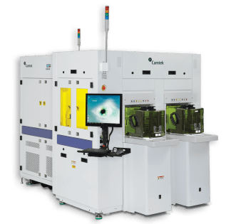
Camtek's Eagle ᵀ - i, designed specifically for speed and accuracy, is one of the fastest and most accurate 2D inspection tools on the market.
This system provides leading 2D inspection capabilities, powered by:
• Genesis detection engine
• New model camera
• New high-end fiber channel model
• Special LED lighting
• Can import CAD design drawings, based on drawing inspection
• Cutting edge processing capability
Eagle ᵀ - i provides advanced solutions for encapsulating applications:
• RDL inspection as low as 2um
• Panel transmission and detection
• Warped wafer transfer and detection
| Inspection Capabilities | Various surface defects inspection of 1 pixel size for Bright Field and 0.5 pixel size for Dark Field |
| Resolution | Multiple magnifications for optimized sensitivity |
| Zone Editing | CAD based detection |
| CAD | Enables running successive scans in one cycle with different focus, magnification, illumination, sensitivity and detection enginea |
| Multi Recipe | Enables running successive scans in one cycle with different focus, magnification, illumination, sensitivity and detection engines |
| Defect Classification / Filtering | Feature based classification |
| Tool Matching | Simple recipe transfer from system to system System to System results matching |
| Bumptypes | Copperpillar,solder,goldbumps,microbumps |
| Capabilities | Measurementofbumpheight,co-planarity,PR/PI thicknessandviaopeningdepthandsurface-to surfacemetrology |
| CTS‒CamtektriangulationSensor:Highspeed3Dscan | |
| HeightAccuracy① | 0.1μm |
| HeightRepeatability① | 1%ofbumpheightand>0.2μmat3σ |
| MeasurementRange | 2‒250μm |
| CCS-CamtekConfocalSensor:3Dhighresolutionprofileareamapping CCS‒Camtek | |
| HeightRepeatability① | 0.1μmat3σ |
| LayerthicknessRange | 5-200μm |
| Heightmetrologyrange | 1μm-300μm |
| CLIP‒CamtekLightinterferometerprofiler: | |
| Resolution | 0.05μm |
| HeightRepeatability① | 0.2μmat3σ |
| MeasurementRange | 0.2-100μm |
| Object types | Bump, RDL, Pad, UBM, Via |
| Capabilities | Measurement of diameter, width, length, placement deviations, overlay, die shift |
| Accuracy | 0.1μm |
| Repeatability | 0.2μm at 3σ |
| Setup Online and Offline | User-defined detection parameters per defect type
and zone. Interactive automated routines for easy zone definition定义 |
| Job Portability & Tool Matching | Allows transfer of jobs between compatible models running on same SW version for system to system results matching |
| Review Options | Color Black & White IR |
| Smart Grab | Customized preset for defect type, count and location, minimizing grabbing and verification time, optimizing image quality to defect type |
| Offline Station | PC-based station for viewing and reclassification of defect images captured during scanning (monochrome) or post-scanning (color and/or monochrome) |
| Histograms | Distribution charts of all defect and metrology data |
| Reports | SPC analysis at lot, wafer and die level, KLARF |
| Wafer Maps | Generate, import, edit and export wafer maps in over 50 standard and custom formats |
| Material Handling Dual Arm Auto Loader | Dual purpose bare & framed on the same load port Supports Bare, Taiko, Framed, Stretched and Reconstructed wafers Bare, Taiko, Framed, Stretched and Reconstructed 4”-12” wafer size |
| Particle Removal System | Removes loose particles, eliminating nuisance calls |
| OCR | Automatic top or bottom wafer ID reading |
| Barcode Reader | Reads data matrix or barcode formats |
| Factory Automation | SECS/GEM or customized host communication; OHT/AGV ready |
| Cleanliness | Semi class 2 according to ISO-150-14644-1 |
①‒Accuracy and repeatability on VLSI step target

 【 WeChat 】
Address:No. 501, Building 01, Northwest District, Suzhou Nano City,
No. 99, Jinjihu Avenue, Suzhou Industrial Park
Hotline:86-0512-62749825
Phone:86-18912625555 Mr Chen
Email:alan.chen@winwintek.com/ wuj@winwintek.com
Copyright © 2026 Win-Win Electronic Technology International Limited Su ICP NO.2025215884-1 Support:HuiCheng