

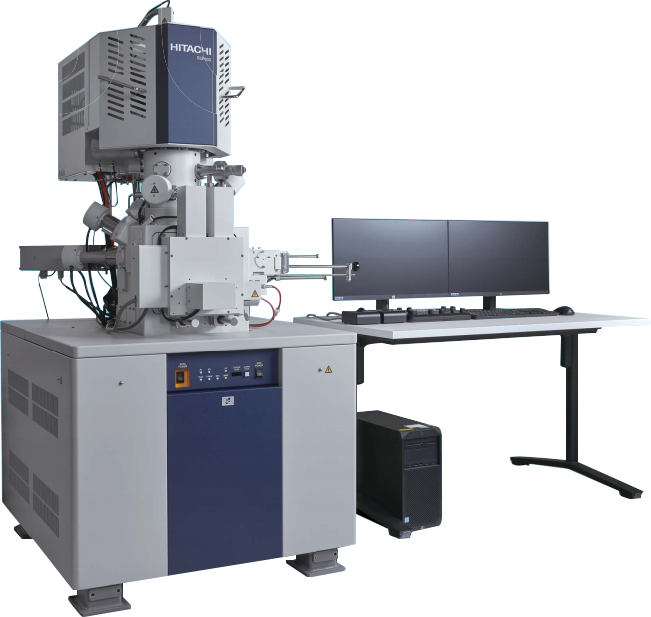
Ultra high resolution field emission scanning electron microscope SU8600 series
With the development of rapid data collection and processing technology, electron microscopes have entered an era where not only data quality but also the collection process are valued. The SU8600 series adheres to the high-quality imaging, large beam analysis, and long-term stable cold field imaging technology of the Regulus 8200 series, while greatly improving high-throughput and automatic data acquisition capabilities.
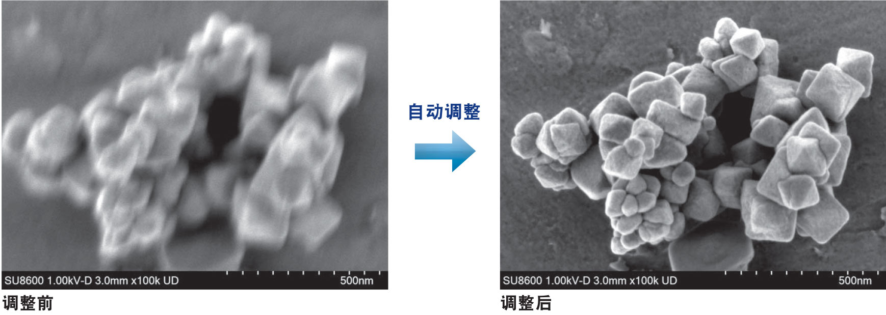
Automatic electronic optical adjustment
Automated data collection for higher detection efficiency.
The use of high-precision piezoelectric sample stages can improve the accuracy of navigation, backtracking, and large-scale continuous imaging.
Equipped with Hitachi's new high brightness cold field emission electron source, ultra-high resolution images can be obtained even at low acceleration voltages.
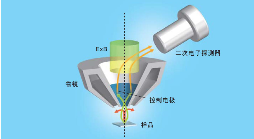
Efficient Signal Acquisition System Based on ExB
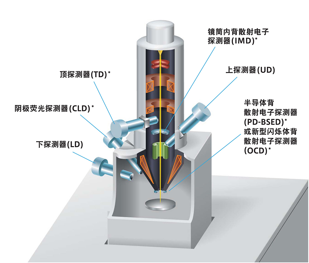
Multiple new electronic detectors and rich optional options to meet more observation needs.
Native support for dual displays, providing flexible and efficient operating space.
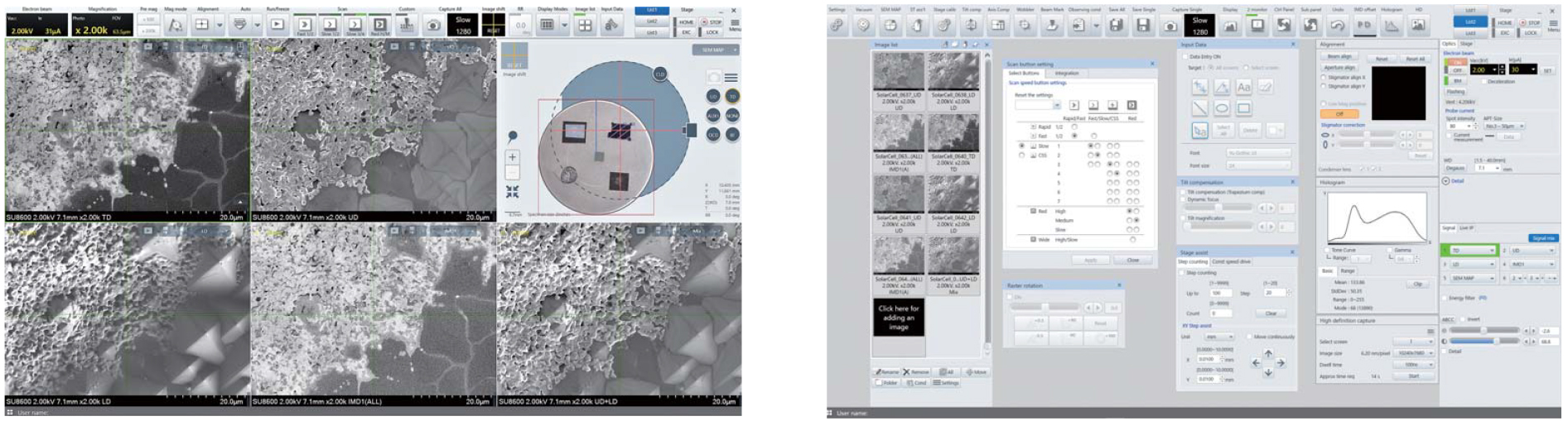
Simultaneously display and save 6 channels to achieve fast multi signal observation and acquisition. Bring more information.
Single scan supports up to 40 Kx30 K ultra-high pixels*
The latest Hitachi High Tech company officially launched a cold field emission electron source in 1972, greatly improving observation resolution. Over the years, we have been dedicated to technological innovation and have never stopped. The instrument adopts the latest electronic gun, which can stably emit electron beams even in high brightness areas. The SU8600 series can obtain high signal-to-noise ratio images even at low acceleration voltages, and the instrument supports long-term testing and high current analysis.

Comparison of SEM Electron Gun Performance
| Cold field emission electron source | Thermal field emission electron source | |
| Electron beam diameter (nm) | 5 | 20 |
| Energy Range (eV) | 0.2~0.3 | 0.6~1.0 |
| Brightness (A/cm2/sr) | 108 | 1078 |
After forming an orthogonal electric and magnetic field (ExBField) above the objective lens, secondary electrons can be efficiently detected without changing the motion trajectory of the incident electrons. Therefore, even with extremely small probe currents, high signal-to-noise ratio and high contrast images can be obtained.
The influence of electric and magnetic fields on incident electrons
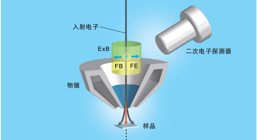
The electric field (E) and magnetic field (B) effects (F) cancel each other out, and the incident electrons do not deflect and can directly pass through the ExB region.
The influence of magnetic field on secondary electrons
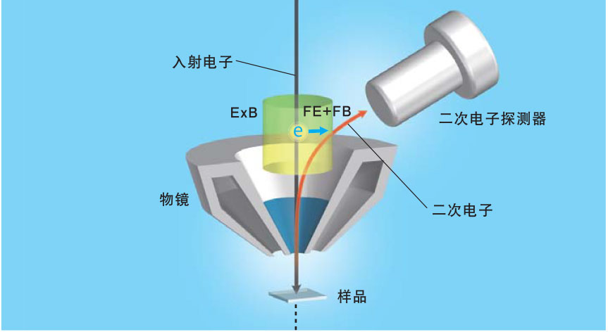
The movement direction of secondary electrons is opposite to that of incident electrons. Under the combined action of electric and magnetic fields, secondary electrons are deflected towards the direction of the secondary electron detector, thereby achieving efficient detection of secondary electrons.
The signal mixing and separation function is a significant feature of Hitachi High Tech's products. By adjusting the voltage of the control electrode in the objective lens, the electrons (secondary electrons or backscattered electrons) reaching the detector can be controlled. Users can obtain a mixed image of secondary electrons and backscattered electrons, easily obtaining the required information.
SE model
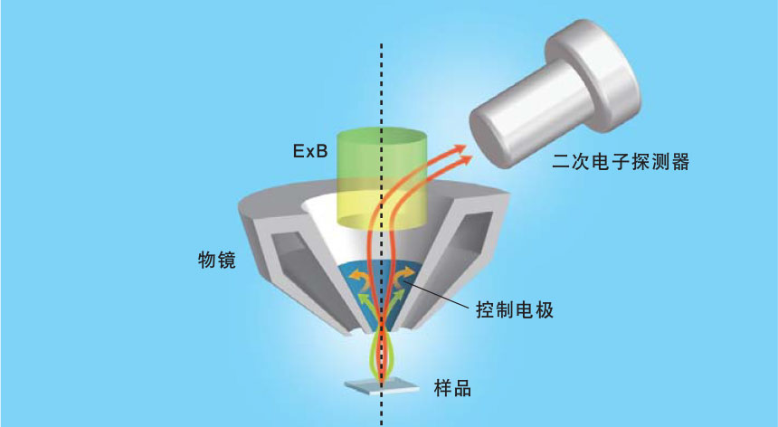
The backscattered electrons are captured by the control electrode, so only the secondary electrons generated by the sample are detected.
LA-BSE model
By adjusting the voltage value of the control electrode, the detection amount of secondary electrons excited from the sample can be controlled. Detect the secondary electrons generated by the impact of backscattered electrons on the control electrode.
● Adopting a new type of cold field emission electron gun with high brightness and stability to achieve ultra-high resolution observation.
● Multiple new detectors are available for selection to meet different application scenarios. (IMD,CLD,PD-BSED,OCD)
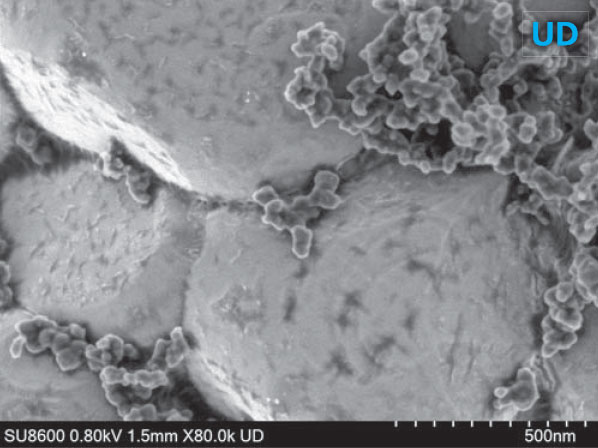
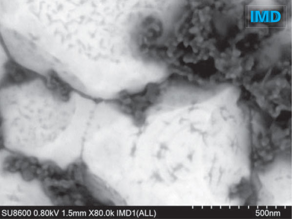
The above three images were obtained simultaneously by three detectors at 0.8kV.
In the UD image, fine structures of metal oxide particles and surface carbon can be observed.
The IMD image shows tiny light element materials distributed on metal oxide particles.
The TD image (on the right) enhances the contrast of elements, revealing another thin layer of light element material covering the metal oxide particles.
Sample: Lithium battery electrode material
Sample provided: DAINEN MATERIALCO. Ltd
Mr. Aoi Yi
EMFlowCreator allows customers to create automated workflows for continuous image acquisition.
EMFlowCreator defines different SEM functions as graphical modules, such as setting magnification, moving sample position, adjusting focal length, and contrast between light and dark.
Users can form a working program by simply dragging and dropping these modules in logical order. After debugging and confirmation, the program can automatically obtain high-quality and reproducible image data every time it is called.
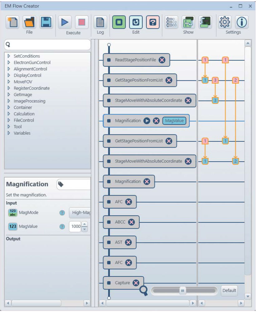
User interface of EM FlowCreator
*
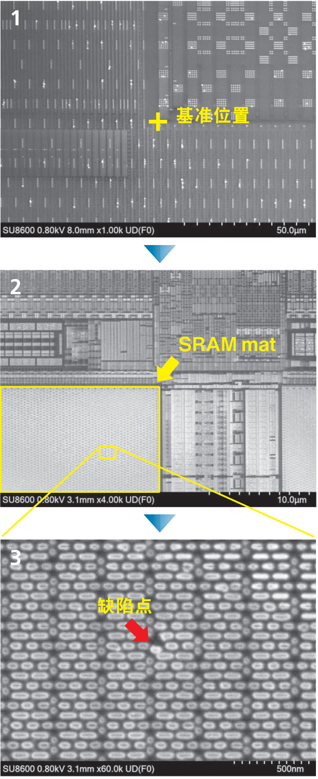
Example of the workflow of EM Flow Creator
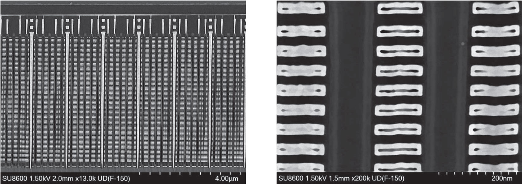
Shoot defects in semiconductor devices:
1. Automatically set SEM observation conditions and move to the reference position.
2. Automatically read the coordinate position recorded in the CSV file and move it to a corner of the SRAMmat area accordingly.
3. Automatically read the coordinate position recorded in the CSV file, move to the defect point, and change the magnification.
*High precision coordinate movement requires the use of a piezoelectric ceramic sample stage
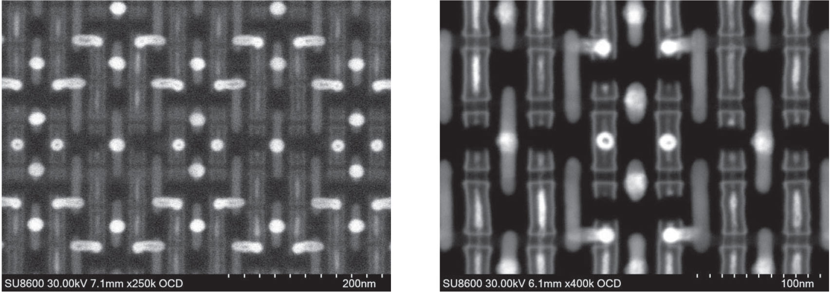
Potential contrast imaging is one of the effective methods for visualizing defects in semiconductor devices. The above image is an observation example of a Contact plug in the SRAM area of a 5nm process. The left image shows the connection layer of w captured using a 0.5kV UD detector, and the right image shows the connection layer of Co-W captured using a 0.3kV TD detector deceleration mode. Choosing appropriate SEM observation conditions can greatly improve the efficiency of obtaining target information in specific samples, such as adjusting landing voltage, switching appropriate detectors and detection conditions, etc.
Left image: Overall 3D NAND cross-section image
Right image: Partial enlarged image. Under low acceleration voltage conditions of 1.5 kV, the backscattered electron signal can clearly show the contrast difference between the silicon oxide layer and the silicon nitride layer.
Left image: The internal structure of Fin FET can be observed. Due to the use of a new type of OCD detector, clear structural images can still be observed even if the photography time is less than 1 second.
Right image: Partially enlarged, the image obtained at normal scanning speed shows excellent signal-to-noise ratio.
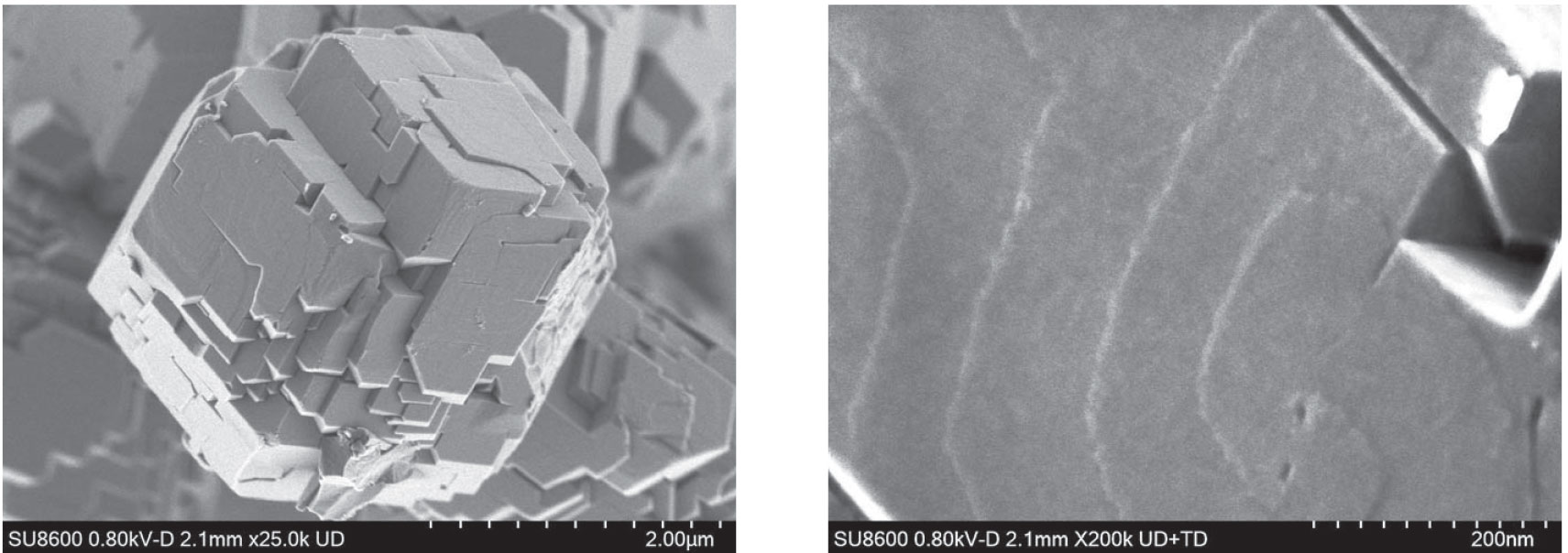
The above is an example of observing RHO zeolite under 0.8kV voltage conditions. The left image shows the overall morphology of the particles, and the right image is an enlarged image. The fine step structure on the surface of the particles is clearly visible. Low voltage observation is more effective in reducing electron beam damage and obtaining surface shape information.
Sample provided by Mr. Yoshida Kamimura from the Japan Institute of Industrial Technology
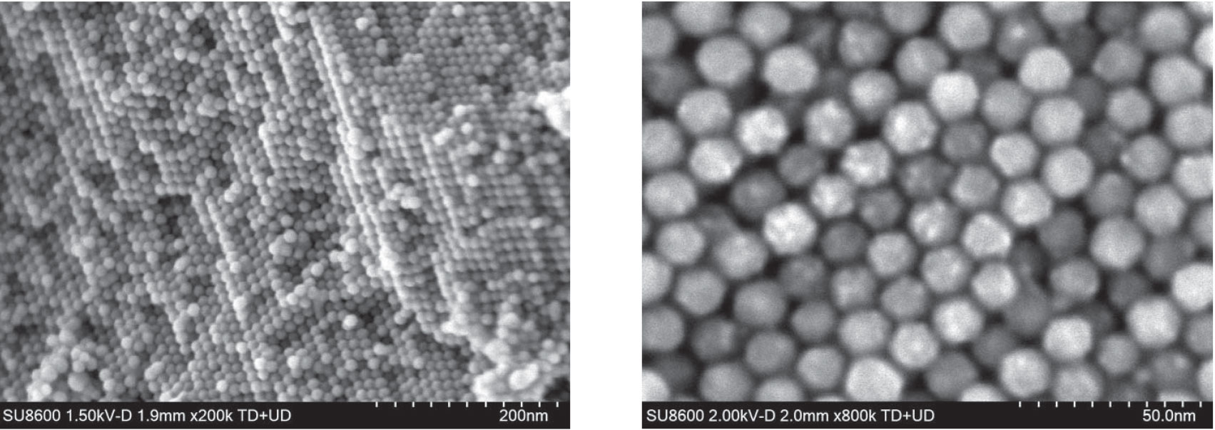
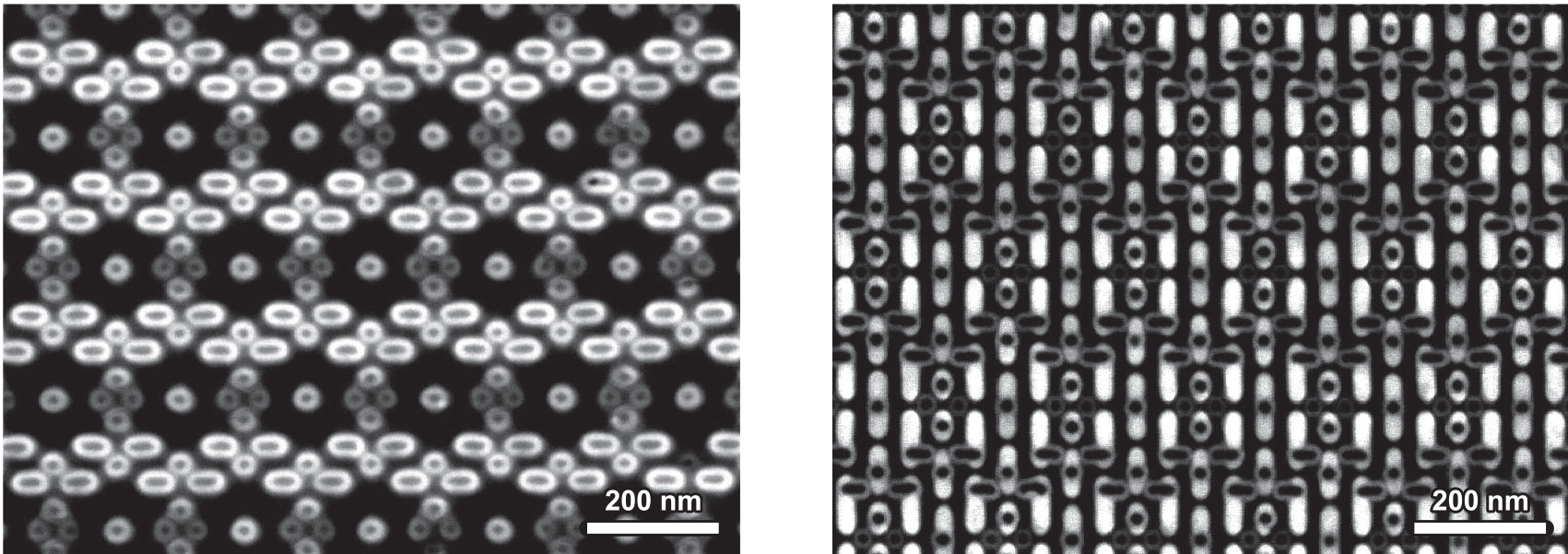
Left image: Neatly arranged self-assembled magnetic nanoparticles of iron oxide
Right image: x800k magnification of the local area, allowing for clear observation of the fine structure on the surface of particles with a diameter of 12nm.
Sample provided: Electrical Computer Engineering Department National University of Singapon
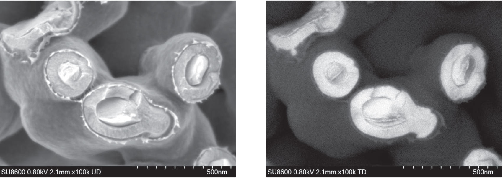
SEM observation of tantalum coating fracture on the surface of capacitor materials. The above image is obtained simultaneously by UD and TD channels, which can simultaneously record surface and component information.
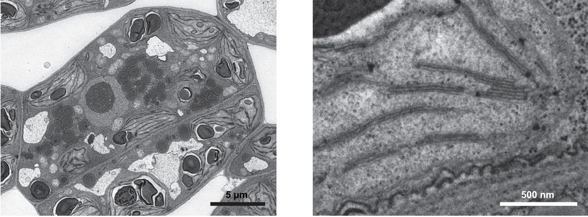
The above image shows the backscattered electron image of ultra-thin slices of mustard leaves in the southern region.
Using a low acceleration voltage of 2kV, an image similar to a TEM image was obtained.
By using energy filtered BSE signals, the ultrastructure of the capsule membrane and other structures can be clearly observed (as shown in the figure on the right).
Sample provided by Mr. Feng Gang from the Environmental Resources Science Research Center and the Institute of Physical Chemistry
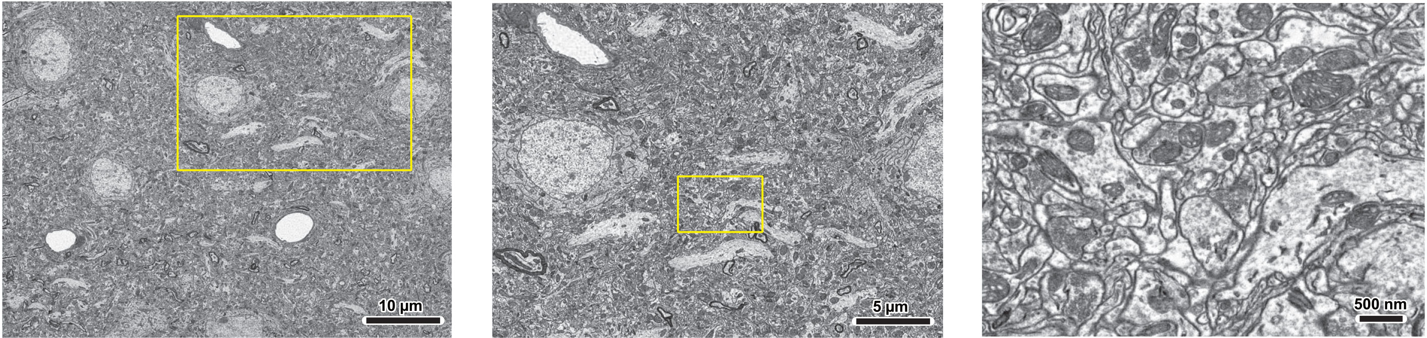
The left image is a high-resolution image of a rat ultra-thin slice sample collected in a single scan with a field of view of approximately 60um.
Enlarge the yellow rectangular area image with simple numbers to obtain the middle image. Continue to enlarge the yellow box in the middle image to obtain the image on the right.
The image on the right is equivalent to a 12 fold digital magnification of the original image on the left, and the internal structure of nerve cell organelles can still be clearly confirmed.
The SU8600 supports high-resolution images up to 40960x30720 pixels in a single scan, as shown above, allowing for a large field of view and high-resolution images.
The above is an example of observing RHO zeolite under 0.8kV voltage conditions. The left image shows the overall morphology of the particles, and the right image is an enlarged image. The fine step structure on the surface of the particles is clearly visible. Low voltage observation is more effective in reducing electron beam damage and obtaining surface shape information.
Sample provided by Mr. Yoshida Kamimura from the Japan Institute of Industrial Technology
Left image: Neatly arranged self-assembled magnetic nanoparticles of iron oxide
Right image: x800k magnification of the local area, allowing for clear observation of the fine structure on the surface of particles with a diameter of 12nm.
Provided by Xiangpin: Electrical Computer Engineering Department National University of Singapon
SEM observation of tantalum coating fracture on the surface of capacitor materials. The above image is obtained simultaneously by UD and TD channels, which can simultaneously record surface and component information.
Channel 1, 2, 4, or 6 signals can be displayed simultaneously on the same monitor, with switchable content including SEM detectors, sample chamber cameras, and navigation cameras.
The workspace can be expanded by using two displays, and the customizable user interface can improve work efficiency.
Can install a sample indoor navigation camera.
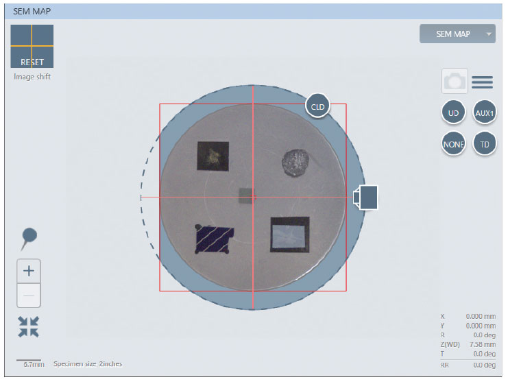
Automatically capture images of the sample stage and transmit them to the SEMMAP screen for easy navigation and quick switching of observation areas.
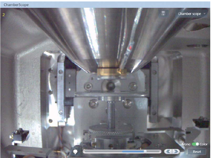
Real time monitoring of the indoor conditions of samples to ensure safe movement of samples in complex situations with multiple attachments. Can switch between color/black and white.
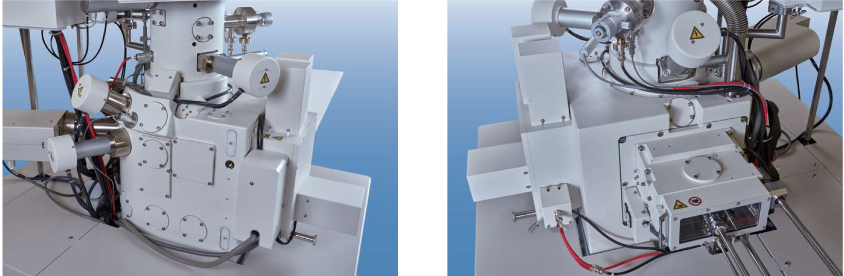
The sample exchange room can accommodate samples with a maximum diameter of 150mm. There are multiple EDS installation interfaces in the sample room.
(The photo includes optional items)
*Optional selection
| Electronic optical system | Secondary electronic resolution | 0.6 nm@15 kV | |
| 0.7 nm@1 kV(1) | |||
| Magnification | 20~2,000,000 x | ||
| Electron gun | Built in cold field emission electron gun and anode heater | ||
| Accelerating voltage | 0.5~30 kV | ||
| Landing voltage (* 1) | 0.01~20 kV | ||
| Sample stage | Motor drive shaft | 5-axis electric motor drive | |
| Mobile range | X | 0~110mm | |
| Y | 0~110mm | ||
| Z | 1.5~40mm | ||
| T | -5~70° | ||
| R | 360° | ||
| Sample room | Sample size | Maximum diameter: 150mm | |
| Detector | Standard detector | Upper detector (UD) (ExB filtering: SE/BSE switchable signal) | |
| Lower detector (LD) | |||
| Optional detector (* 2) | Top detector (TD) | ||
| In tube backscattered electron detector (IMD) | |||
| Scintillator backscattered electron detector (OCD) | |||
| Semiconductor backscattered electron detector (PD-BSED) | |||
| Cathodic Fluorescence Detector (CLD) | |||
| STEM detector | |||
| Optional accessories (* 3) | X-ray energy spectrometer (EDS) | ||
| Electron backscatter diffraction detector (EBSD) | |||
| Image display mode | Large window display mode | 1280x960 pixels | |
| Single image display mode | 800x600 pixels | ||
| Dual image display mode | 800x600 pixels, or use dual displays with 1.280x960 pixels | ||
| Four image display modes | 640x480 pixels | ||
| Six image display modes | 640x480 pixels (using dual displays) | ||
| Shooting pixels | 640480 1,280960 2,5601,920 5,1203,840 10,2407,680 20,48015,360(*2)40,960x30,720(*2) | ||
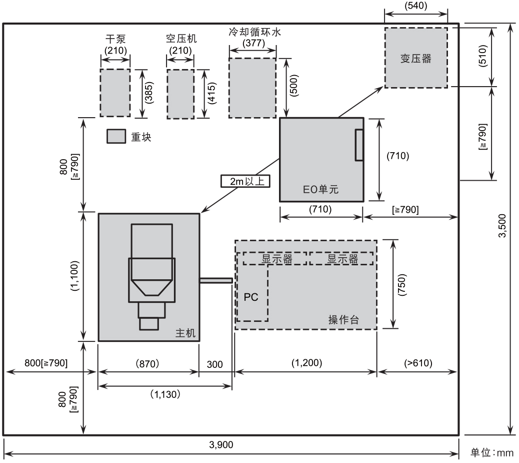
| Volume and weight (* 4) | Host | 1130 (W) x1100 (D) x1750 (H) mm, approximately 660kg | |
| EOC Unit | 710(W)x710(D)x1,210(H)mm,approximately 260 kg | ||
| Heavy block | 200(W)x160(D)x140(H)mm,approximately 25 kg | ||
| Installation requirements | Room temperature | 15~25℃ | |
| Humidity | Below 60% (RH) (no condensation) | ||
| Power supply (host) | AC100 V10 %,4kVA | ||
| Power Supply (CT-6020) | AC100 V10 %,1.5kVA | ||
| Grounding | 100 Ω or below | ||
| Cooling circulating water | Recommend using a dedicated cooling circulating water device (* 5) | ||
| Vacuum pump | Dry pump (* 5) | ||
| Air compressor (* 6) | 600~800 kPa | ||
(* 1) In deceleration mode
(* 2) Optional
(* 3) Installed analyzer detector.
(* 4) The weight is the standard host weight and does not include optional items.
(* 5) Provided by the customer
(* 6) When connecting with customer devices

 【 WeChat 】
Address:No. 501, Building 01, Northwest District, Suzhou Nano City,
No. 99, Jinjihu Avenue, Suzhou Industrial Park
Hotline:86-0512-62749825
Phone:86-18912625555 Mr Chen
Email:alan.chen@winwintek.com/ wuj@winwintek.com
Copyright © 2026 Win-Win Electronic Technology International Limited Su ICP NO.2025215884-1 Support:HuiCheng