

Support large-scale sample testing
Combining excellent performance, easy operation, and diverse functions; Configure multiple operation assistance functions to support a series of processes from sample installation to testing; With the enhancement of various automation functions, operational performance has been further optimized; A detector that can meet various observation needs; Equipped with a multifunctional oversized sample compartment as standard, supporting analysis of large samples; Support full field of view movement, SEM MAP supports full field of view observation of oversized samples; Can provide application solutions that meet testing requirements; Equipped with a multifunctional oversized sample compartment and a wide range of accessories
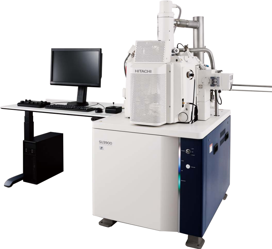
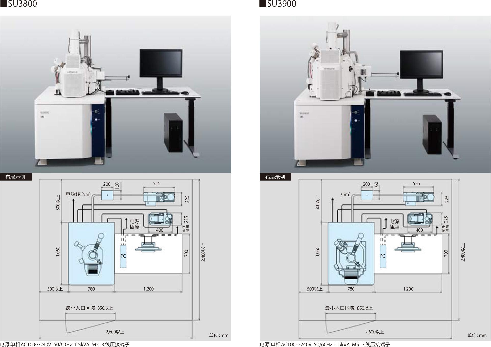
The scanning electron microscope SU3800/SU3900 launched by Hitachi High Tech combines operability and scalability, and with numerous automation functions, can efficiently unleash its high performance. SU3900 comes standard with a multifunctional oversized sample compartment, which can handle the observation of large samples.
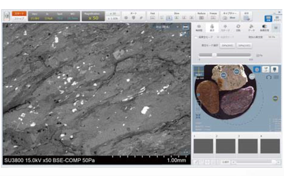
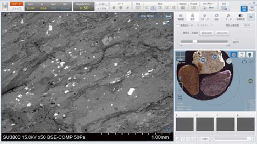
This product uses a validated GUI interface. In addition, it is equipped with the highly acclaimed SEMMAP, and the camera navigation system provides a large field of view navigation, providing operators with a more intimate and smooth operating experience.
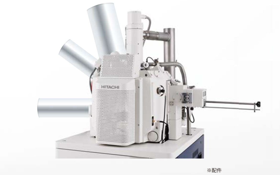
Equipped with a multifunctional oversized sample compartment, it can carry a variety of accessories.
And it is also applicable to large samples with diameters of 200mm (SU3800) and 300mm (SU3900).
By replacing the sample prompt, it is possible to prevent damage to the equipment or sample due to contact with the sample.

By using the automatic start function and automatic optical axis adjustment function, it is possible to quickly observe.

The wide-angle camera navigation covers the entire area of the maximum observation zone.

You can easily find the target observation object.

In addition to the integrated EDS function, it can also be used in conjunction with other devices and software. One key switch between high and low vacuum, no need to manually install differential pressure diaphragm; Equipped with an air compressor and fully automatic air valve control.

SEM/EDS/SEM MAP images can be uniformly arranged in any layout, and personalized reports can be output according to requirements.

Comes standard with a large multifunctional sample compartment. Can support In Situ analysis.
Equipped with a minimalist GUI, simple operation, as intuitive as a touch screen.
● From moving the sample stage to observing the sample, simply click the mouse lightly to achieve it.
● It can also be operated through touch screen.
● The main window is a large window with 1280x960 pixels.
● It can switch display modes and simultaneously display/capture two different signals.
You can move the field of view by clicking or dragging anywhere on the real-time image. It can delineate any position on the real-time image, and the delineated position can be moved to the center of the field of view and enlarged.

Any signal can be displayed or loaded simultaneously in the GUI.

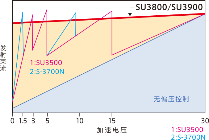
The HexBias automatic bias and fixed six level bias functions of the electron gun ensure beam current and obtain high-quality images under low acceleration voltage.
High resolution SE image
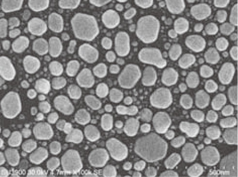
Sample: Vapor deposited particles of gold
Observation image of low acceleration voltage

Sample: CFRP
UVD imaging*
Sample: Paint on filter
Low vacuum observation image
Sample: Paint on filter
*Accessories
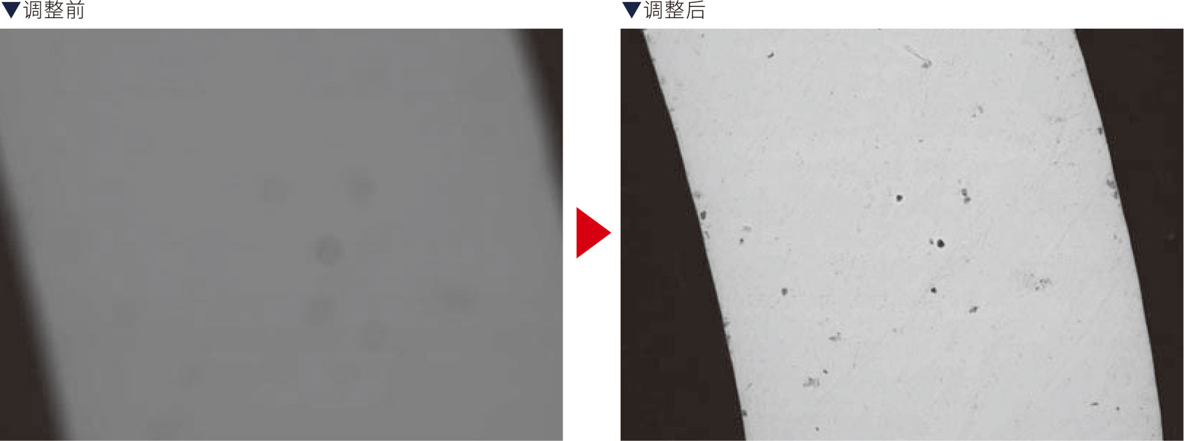
The various adjustment tasks required for adjusting the optical axis and replacing the filament have been automated. This can suppress the deviation between the optical axis and the field of view, so that high-quality data can be obtained with good reproducibility without relying on the skills of the operator.

The SU3800/SU3900 is equipped with automatic adjustment functions for electronic optical systems and detection systems.
After placing the sample and vacuuming, the image can be automatically adjusted through the automatic start function, and clear images can be obtained immediately after electron beam irradiation.
The highly automated function adopts a newly designed calculation program, which reduces the waiting time to less than one-third of the previous when performing image automatic adjustment functions. No need for tedious portrait adjustments, high-throughput image data can be easily obtained.

The newly upgraded automatic focus adjustment function makes it easier to obtain images even for smooth samples that were previously difficult to adjust.
Equipped with Intelligent Filament Technology (IFT)
● Automatically monitor the status of the filament and control it to maintain optimal performance at all times.
● Equipped with a display screen that shows the filament replacement time.
Through this feature, large-scale analysis such as long-term continuous observation and data analysis that were previously difficult to correspond to can be achieved with peace of mind.

The SU3800/SU3900 has expanded its vacuum mode and detection capabilities to meet diverse observation needs. In addition to being able to install secondary electron detectors and high-sensitivity semiconductor backscattered electron detectors that can operate in any vacuum mode, UVD can also be installed. UVD can obtain the concave convex information of the sample and the cathodoluminescence (CL information) generated by electron beam irradiation.

The SU3800/SU3900 are equipped with high-sensitivity low vacuum detectors UVD. In addition to the concave convex image on the surface of the sample, CL information can also be obtained by detecting the cathodoluminescence generated by electron beam irradiation on the sample.

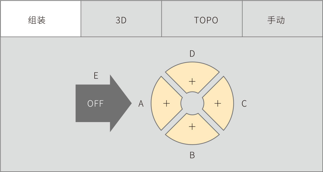
By adopting a design of 4 divisions+1 unit, calculations can be performed for each unit without tilting the sample, resulting in component images, 3D images, and 4-directional concave convex images.
Due to the exquisite design and high sensitivity of the detector, high resolution and high signal-to-noise ratio have been achieved.

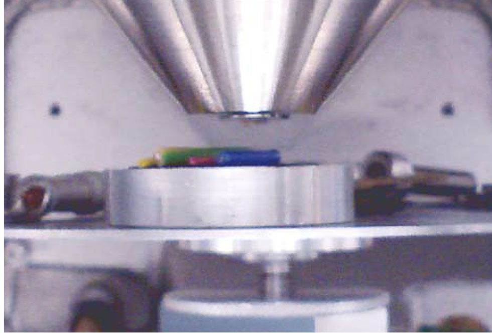
SU3800/SU3900 are equipped with sample tables that support oversized/overweight samples

| SU3800 | SU3900 | |
| Maximum sample size | Diameter 200mm | Diameter 300mm |
| Maximum observable range | Diameter 130mm | Diameter 200mm |
| Maximum allowable weight | 2kg | 5kg(without TZR) |
| Maximum height that can be carried | 80mm | 130mm |

The operation steps for replacing the sample are displayed on the GUI. It can avoid sample contamination or damage caused by human error. Even uneven or oversized samples that are difficult to detect can be easily replaced.

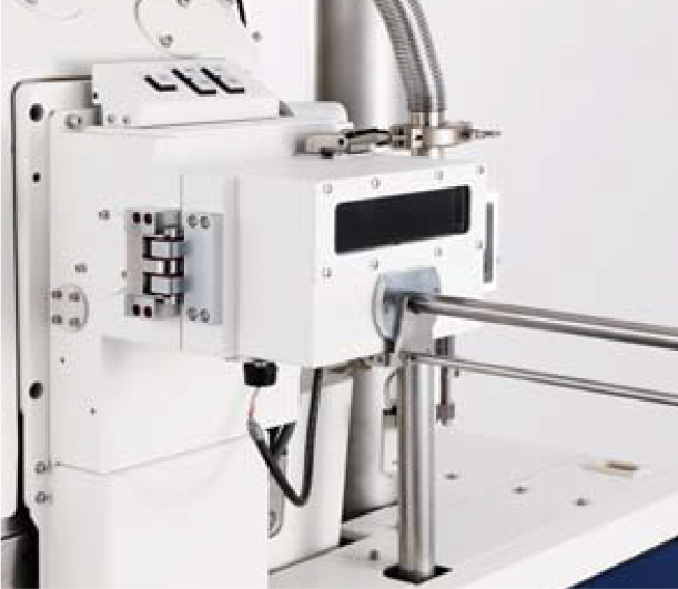
The optional sample exchange chamber allows for quick replacement of samples while maintaining a vacuum in the main sample chamber, greatly improving work efficiency.
Infrared CCD detector is a device used to monitor the interior of the sample chamber. By using an infrared camera, it is possible to monitor the inside of the sample chamber while observing SEM images. To obtain a more detailed position, the CCD image can be enlarged and the observation position can be moved.
The SU3800/SU3900 can be equipped with a device table movement restriction release function that can improve the freedom of device table movement. According to the operator's judgment, the device table can move freely.
The device platform movement restriction release function can be used when equipped with a chamber oscilloscope.
The Zigzag function can automatically obtain a continuous field of view. Multi Zigzag can set Zigzag in multiple areas of the sample stage, capture multiple high magnification images in different fields of view, and use the Viewer function to stitch the captured images to create a large field of view image.
SEM MAP combined with GUI realizes wide-angle camera navigation *. By specifying the observation target position on the SEM MAP, it can be smoothly moved to the designated location. Images captured using the large field camera navigation system or external images can be freely zoomed in or out to switch from large field color images to high magnification SEM images.

The camera navigation system can achieve SEM MAP observation with a large field of view through image stitching function. The observation area is Diameter 127mm (SU 3800)/Diameter 200mm (SU3900), and can be linked with the sample stage R to move to the maximum observation area of large samples.

The SEM MAP operation interface can intuitively display the position relationship between the sample and the detector. Therefore, when observing samples with large height differences, the sample stage or electron beam can be rotated according to the needs to obtain the optimal observation and analysis position, avoiding the influence of shadow effects.

The newly developed SEM/EDS integrated function of SU3800/SU3900 can complete a series of operations such as determining test positions, setting conditions, analyzing samples, and generating reports through the SEM operation interface. By controlling SEM, testing efficiency can be improved and the burden on operators can be reduced.

For detailed analysis of higher functionality, it can be linked to EDS-GUI for analysis. Simply click on the icon to seamlessly switch with EDS-GUI.
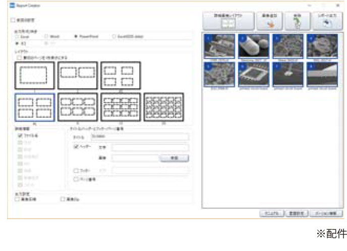
In Report Creator, SEM images, EDS data, CCD camera images, and other collected images can be integrated to generate a report. The created report can be saved in Microsoft Office format. The saved file can be edited through Microsoft Office.
Hitachi map 3D can perform computational analysis on SEM signals from four different directions in the 5-segment backscattered electron detector SU3800/SU3900, generating three-dimensional images. Support measurement of height, volume, and simple surface roughness (surface roughness, line roughness) between 2 points. It can receive signals from four different directions at once, so there is no need to tilt the sample stage or synthesize images.

The SU3800/SU3901 is equipped with IPl and can transfer SEM images to ImagePro, an image processing software developed by Media Cybernetics in the United States. Just click once to transfer data from SEM to image measurement software.

SU3800/SU3900 can be equipped with STEM holder, which can obtain clear STEM images under high-speed scanning

By heating the sample on a heating table, the dynamic changes of the sample can be observed in situ.

Microtest300 (produced by Gatan) can be used to apply pressure to the sample in the sample chamber to observe dynamic changes.

Reverse osmosis membranes (RO membranes) have the property of being permeable to water but impermeable to impurities such as salts. There is a skin layer on the surface of the reverse osmosis membrane, which plays an important role in separating salt and water. There are numerous protrusions on the surface of the skin layer. Through observation, it can be observed that these protrusions expand when wet, but contract in a vacuum environment (a, b).
Dropping an ionic aqueous solution (5%) onto the reverse osmosis membrane that expands due to distilled water, soaking for 4 hours, removing excess ionic liquid solution, and conducting SEM observation, it can be observed that the skin layer maintains an expanded state even under high vacuum (c, d).
(a) Dry ion layer (5000 times)

(b) Dry skin layer (20000 times)

(c) The swollen skin layer (5000 times)

(d) Pengrun state skin layer (20000 times)

Accelerated power plant: 7.0kV
Signal: SE
Observation magnification: (a), (c) x5000
Observation magnification: (b), (d) x20000
Tilt of the loading platform: 70
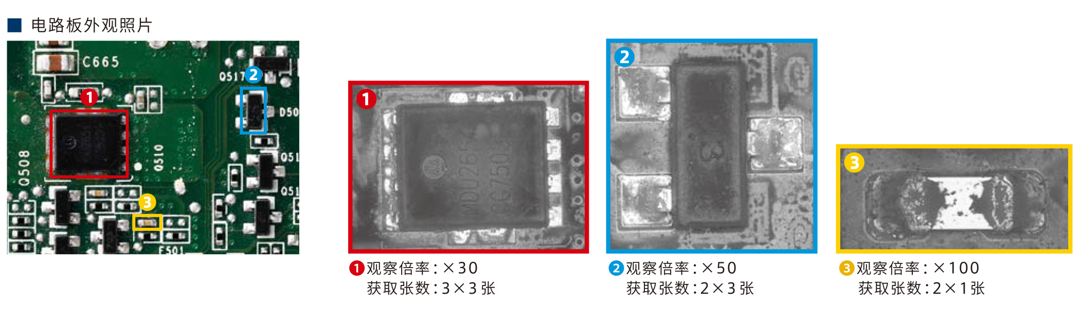
This is an example of cross-sectional analysis of electronic components made by ion milling after mechanical polishing. (a) Multiple layers of copper plating can be confirmed through clear crystal orientation. (b) It can be clearly seen that Ag particles are distributed in the alloy layer and Pb free solder particles at the copper plating/solder grain boundary.
(a) Observe the cross-section of the copper plated part

Acceleration voltage: 5.0kV
Signal: BSE-COMPO
Observation magnification: X25000
(b) Observe the cross-section at the copper plating/soldering grain boundary

Acceleration voltage: 5.0kV
Signal: BSE-COMPO
Observation magnification: x25000
The Hitachi composite ion grinder ArBlade 5000 can perform pre-treatment of required samples through both cross-sectional and planar grinding. In section grinding, the protruding edge (local sample) is sputtered along the edge of the shielding plate to obtain a uniformly cut section. In planar grinding, offsetting (eccentric adjustment) the ion beam from the center of rotation of the sample can achieve a wide range of processing that is difficult to achieve in cross-sectional grinding.

Carbon fiber reinforced plastic (CFRP) is a composite material made by overlapping carbon fibers and curing them with resin, characterized by lightweight and high strength. (a) Can confirm the resin distribution around the carbon fiber. (b) The CFRP section processed by an ion grinder shows that carbon fibers and resin adhere tightly to each other in both longitudinal and transverse directions without any gaps.
(a) Observe the surface of CFRP

Acceleration voltage: 7.0 kV
Signal: UVD
Observation magnification: x25000
(b) Observing CFRP cross-section

Acceleration voltage: 7.0 kV
Signal: BSE-COMPO
Observation magnification: X250
It is very important to repeatedly observe the machined surface to confirm the machining status in the pretreatment by ion milling. By using a connecting rod bracket, the processing status can be checked without removing the sample.

The observation results of zircon crystals under the same field of view are displayed. It is difficult to distinguish the moderate deviation of zirconium concentration in BSE images. However, it can be confirmed in the CL image that the dark areas correspond to regions with higher zirconium concentration.

Titanium material

Acceleration voltage: 5kV
Observation magnification: x800
Metal fracture surface

Acceleration voltage: 7kV
Observation magnification: x10000
VTiO2

Acceleration voltage: 8kV
Observation magnification: x50000
Al2O3

Acceleration voltage: 8kV
Observation magnification: X32000
Adhesive surface

Acceleration electric vehicle: 15kV
Observation magnification: X550
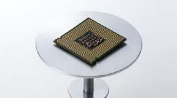
Electronic component

Acceleration voltage: 15kV
Observation magnification: x15
Mold

Acceleration voltage: 4kV
Observation magnification: x470
Mold

Acceleration voltage: 1.2kV
Observation magnification: X5000
Mold

Acceleration voltage: 4kV
Observation magnification: x470
Mold

Acceleration voltage: 1.2kV
Observation magnification: X5000
Kidney section

Acceleration voltage: 30kV
Observation magnification: x1300
Liver slice

Acceleration voltage: 30kV
Observation magnification: X25000
Tablet

Acceleration electric power: 20kV
Observation magnification: X7
Algae

Acceleration voltage: 8kV
Observation magnification: 1300
| ITEM | SU3800 | SU3900 | |
| Secondary electron decomposition energy | 3.0nm (acceleration voltage 30kV, WD=5mm, high vacuum mode) | ||
| 15.0nm (acceleration voltage 1kV, WD=5mm, high vacuum mode) | |||
| Backscattered electron decomposition energy | 4.0nm (acceleration voltage 30kV, WD=5mm, low vacuum mode) | ||
| Magnification | X5~x300, 000 (photo magnification * 1) | ||
| X7~800, 000 (actual display magnification * 2) | |||
| Accelerating voltage | 0.3kV~30kV | ||
| Low vacuum setting | 6~650 Pa | ||
| Image displacement | 土50um(WD=10mm) | ||
| Maximum sample size | 200mmDiameter | 300mmDiameter | |
| Sample stage | X | 0~100mm | 0~150mm |
| Y | 0~50mm | 0~150mm | |
| Z | 5~65mm | 5~85mm | |
| R | 360 ° continuous | ||
| T | -20°~+90° | ||
| Maximum observable range | 130mm Diameter (R combined) | 200mmDiameter (R combined) | |
| Maximum observable height | 80mm(WD=10mm) | 130mm(WD=10mm) | |
| Motor drive | 5-axis motor drive | ||
| Electronic optical system | Electron gun | Central controlled tungsten wire emission | |
| Image lens aperture | 4-hole movable aperture | ||
| Detection system | Secondary electron detector, high-sensitivity semiconductor backscattered electron detector | ||
| EDX analysis WD | WD=10mm(T.0.A=35°) | ||
| Image display | Automatic optical axis adjustment function | Automatic Beam Adjustment (AFSABAAFCABCC) | |
| Automatic optical axis adjustment (real-time level alignment) | |||
| Automatically adjust beam brightness | |||
| Automatic image adjustment function | Automatic Brightness and Contrast Control (ABCC) | ||
| Automatic Focus Control (AFC) | |||
| Automatic Marking and Focus Function (ASF) | |||
| Automatic Filament Saturation Adjustment (AFS) | |||
| Automatic Beam Alignment (ABA) | |||
| Automatic Start (HV-ONABCCAFC) | |||
| Operation assistance function | Optical rotation, dynamic focusing, image quality improvement function, data input (point-to-point measurement, angle measurement, text), preset magnification, sample stage position navigation function (SEMMAP), beam marking function | ||
| Accessories | Hardware: trackball, joystick, control panel, compressor, high-sensitivity low vacuum detector (UVD), infrared CCD detector, camera navigation system Software: SEM data manager external communication interface, 3D capture, device platform movement restriction release function, EDS integration | ||
| Accessories (external devices) | Energy dispersive X-ray analyzer (EDS), wavelength dispersive X-ray analyzer (WDS), various external functional stations (heating station, cooling station, traction station) | ||
*1: Specify a display size with a magnification of 127mmx95mm (4x5 photo size). *2: Specify a display size with a magnification of 509.8mmx286.7mm (1920x1080 pixels).

 【 WeChat 】
Address:No. 501, Building 01, Northwest District, Suzhou Nano City,
No. 99, Jinjihu Avenue, Suzhou Industrial Park
Hotline:86-0512-62749825
Phone:86-18912625555 Mr Chen
Email:alan.chen@winwintek.com/ wuj@winwintek.com
Copyright © 2026 Win-Win Electronic Technology International Limited Su ICP NO.2025215884-1 Support:HuiCheng