

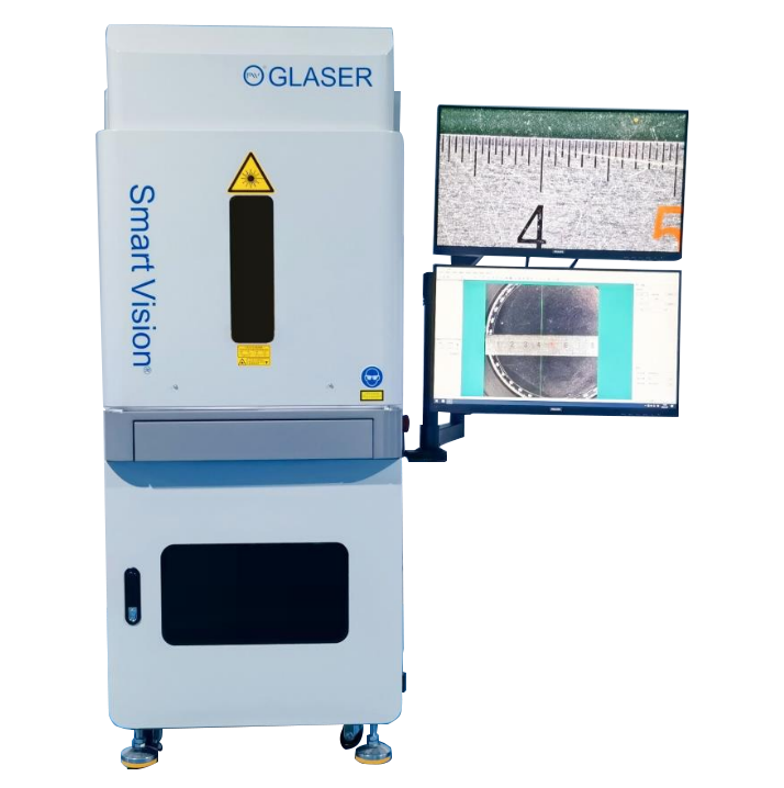
In the analysis of semiconductor chip failure, precise etching, precise layer cutting, failure point positioning, precise opening, stress free etching, and precise thinning before chemical etching can be achieved, which is clean and environmentally friendly. It is a powerful tool assistant for chip failure analysis engineers, improving analysis efficiency. Laser etching belongs to dry etching, which is currently the only non-destructive and flexible processing technology. For the non-destructive etching of metal wires inside chips, some analysis does not require chemical etching. This layer cutting process can be used for flexible two-dimensional and three-dimensional contour processing, achieving 3D subtractive printing. The camera function can be used to correct the misalignment between the laser and the observation light beyond the center of the scanning area, so that the focal position appearing in the image is consistent with the actual position of the laser focal point, achieving the effect of what you see is what you get.
● The perfect combination of laser and vision, coaxial confocal imaging, and vertical imaging.
● Concise user interface
● Easy to use and learn
● Professional Kaifeng Software
● Foolish attempt to draw graphics
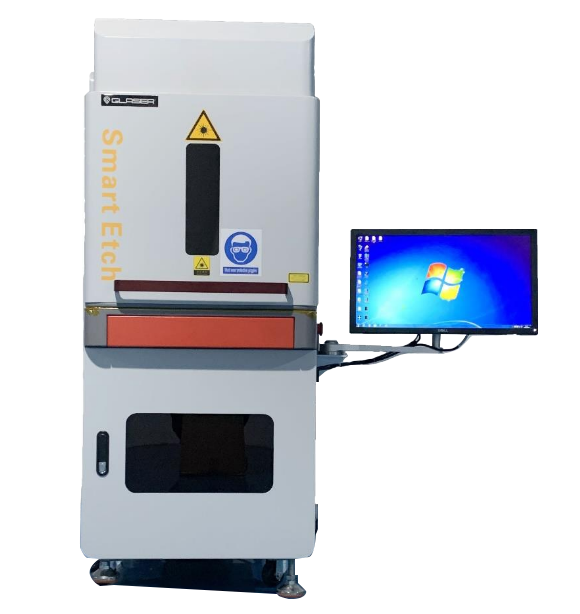
● Provide ultra stable laser opening process
● No damage to the wires
● Suitable for opening copper, gold, silver and other bonding wires
● Real time visibility of the opening process
● The perfect combination of laser and vision.
● Concise user interface
● Easy to use and learn
● Professional Kaifeng Software
● Foolish attempt to draw graphics
● Provide ultra stable laser opening process
● No damage to the wires
● Suitable for opening copper, gold, silver and other bonding wires
● Real time visibility of the opening process

 【 WeChat 】
Address:No. 501, Building 01, Northwest District, Suzhou Nano City,
No. 99, Jinjihu Avenue, Suzhou Industrial Park
Hotline:86-0512-62749825
Phone:86-18912625555 Mr Chen
Email:alan.chen@winwintek.com/ wuj@winwintek.com
Copyright © 2026 Win-Win Electronic Technology International Limited Su ICP NO.2025215884-1 Support:HuiCheng